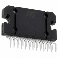
TDA7382 STMicroelectronics, TDA7382 Datasheet

TDA7382
Specifications of TDA7382
Related parts for TDA7382
TDA7382 Summary of contents
Page 1
... S designed for high end car radio applications. Thanks to the fully complementary PNP/NPN out- put configuration the TDA7382 allows a rail to rail output voltage swing with no need of bootstrap capacitors. The extremely reduced components count allows very compact sets. The on-board clipping detector simplifies gain compression op- erations ...
Page 2
... TDA7382 ABSOLUTE MAXIMUM RATINGS Symbol V Operating Supply Voltage Supply Voltage CC (DC) V Peak Supply Voltage (t = 50ms) CC (pk) I Output Peak Current: O Repetitive (Duty Cycle 10 10Hz) Non Repetitive (t = 100 s) P Power dissipation, (T tot T Junction Temperature j T Storage Temperature stg PIN CONNECTION (Top view) 1 THERMAL DATA ...
Page 3
... THD = 10 14V S THD = 5 14V S THD = 1 14V S THD = 10 13.2V S THD = 1 13.2V S EIAJ RULES "A" Weighted Bw = 20Hz to 20KHz f = 100Hz f = 1KHz St-By = LOW (Amp: ON) (Amp: OFF 1Vrms O (Amp: Play) (Amp: Mute 1.5V MUTE (Source Current) TDA7382 = amb Min. Typ. Max. Unit 85 180 300 mA 100 16 ...
Page 4
... TDA7382 Figure 1: Standard Test and Application Circuit R1 ST-BY 10K MUTE 47K C10 IN1 0.1 F IN2 C2 0.1 F IN3 C3 0.1 F IN4 C4 0.1 F S-GND 4/ 0.1 F 2200 F Vcc1-2 Vcc3 SVR CLIPPING DET TAB D98AU819 OUT1 OUT2 OUT3 OUT4 ...
Page 5
... Figure 2: P.C.B. and component layout of the figure 1 (1:1 scale) COMPONENTS & TOP COPPER LAYER BOTTOM COPPER LAYER TDA7382 TDA7382 5/10 ...
Page 6
... TDA7382 Figure 3: Quiescent Current vs. Supply Voltage Figure 5: Output Power vs. Supply Voltage Figure 7: Distortion vs. Frequency. 6/10 Figure 4: Quiescent Output Voltage vs. Supply Voltage Figure 6: Distortion vs. Output Power Figure 8: Supply Voltage Frequency by varying 600 1Vrms ripple Rejection vs. ...
Page 7
... Figure 9: Output Noise vs. Source Resistance INPUT STAGE The TDA7382’S inputs are ground-compatible and can stand very high input signals ( 8Vpk) without any performances degradation. If the standard value for the input capacitors (0 adopted, the low frequency cut-off will amount to 16 Hz. ...
Page 8
... R-C networks and realize a volume (or tone bass) stepping down in associa- tion with microprocessor-driven audioprocessors. The maximum load that pin 25 can sustain is Figure 12: Diagnostics circuit Vpin 25 TDA7382 D97AU810 Figure 14: Diagnostics Waveforms. ST-BY PIN VOLTAGE MUTE PIN VOLTAGE Vs OUTPUT ...
Page 9
... TDA7382 OUTLINE AND MECHANICAL DATA Flexiwatt25 FLEX25ME D 9/10 ...
Page 10
... TDA7382 Information furnished is believed to be accurate and reliable. However, STMicroelectronics assumes no responsibility for the consequences of use of such information nor for any infringement of patents or other rights of third parties which may result from its use. No license is granted by implication or otherwise under any patent or patent rights of STMicroelectronics. Specification mentioned in this publication are subject to change without notice ...


