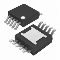
MAX3268CUB+ Maxim Integrated Products, MAX3268CUB+ Datasheet

MAX3268CUB+
Specifications of MAX3268CUB+
Related parts for MAX3268CUB+
MAX3268CUB+ Summary of contents
Page 1
... V CC MAX3266 MAX3267 Typical Operating Circuits continued at end of data sheet. ________________________________________________________________ Maxim Integrated Products For pricing, delivery, and ordering information, please contact Maxim/Dallas Direct! at 1-888-629-4642, or visit Maxim’s website at www.maxim-ic.com. +3.0V to +5.5V, 1.25Gbps/2.5Gbps ♦ +3.0V to +5.5V Supply Voltage ♦ Low Deterministic Jitter ...
Page 2
Limiting Amplifiers ABSOLUTE MAXIMUM RATINGS Supply Voltage (V ) ............................................-0.5V to +6.0V CC Voltage at IN+, IN- ..........................(V CC Voltage at SQUELCH, CAZ1, LOS, TH..................................-0. CAZ2, LOS, Voltage at LEVEL...................................................-0.5V to +2.0V Current into ...
Page 3
ELECTRICAL CHARACTERISTICS (continued) (Data outputs terminated per Figure 1, V unless otherwise noted.) (Note 1) PARAMETER Medium LOS Assert Level R TH Medium LOS Deassert Level R TH High LOS Assert Level R TH High LOS Deassert Level R TH ...
Page 4
Limiting Amplifiers ELECTRICAL CHARACTERISTICS—MAX3265EUE (Data outputs terminated per Figure 1, V unless otherwise noted.) (Note 1) PARAMETER Data Rate Input Voltage Range Deterministic Jitter (Notes 2, 3) Random Jitter (Notes 2, 4) Data Output Edge Speed ...
Page 5
A OUTPUT VOLTAGE vs. INPUT VOLTAGE 1700 1500 MAX3264/MAX3268 1300 1100 MAX3265/MAX3269/MAX3765 900 700 500 300 INPUT VOLTAGE (mV) MAX3264/MAX3268/MAX3768 DETERMINISTIC JITTER vs. INPUT AMPLITUDE ...
Page 6
Limiting Amplifiers (T = +25°C, unless otherwise noted.) A MAX3264 DATA OUTPUT EYE DIAGRAM AT 1.25Gbps (MINIMUM INPUT) 150mV/div 200ps/div MAX3265/MAX3765 DATA OUTPUT EYE DIAGRAM 2.5Gbps (MAXIMUM INPUT) 150mV/div 100ps/div MAX3264 LOSS-OF-SIGNAL THRESHOLD vs ...
Page 7
PIN NAME µMAX TSSOP GND LOS 11 OUT OUT+ — 1 CAZ1 ...
Page 8
Limiting Amplifiers 100Ω 100Ω 100Ω MAX3264 MAX3265 MAX3765 (a) MAX3264/MAX3265/MAX3765 WITH 50Ω TERMINATION MAX3268 MAX3269 MAX3768 (c) MAX3268/MAX3269/MAX3768 OUTPUT TERMINATION Figure 1. Data Output Termination 8 _______________________________________________________________________________________ R TERM 100Ω 100Ω C ...
Page 9
MAX3264 MAX3265 MAX3765 (a) CML SUPPLY CURRENT (I (b) PECL SUPPLY CURRENT (I Figure 2. Power-Supply Current Measurement _______________________________________________________________________________________ +3.0V to +5.5V, 1.25Gbps/2.5Gbps 100Ω 100Ω CONTROL R TH 2.5kΩ OUT+ ...
Page 10
Limiting Amplifiers _______________Detailed Description Figure functional diagram of the MAX3264/ MAX3265/MAX3268/MAX3269/MAX3765/MAX3768 lim- iting amplifiers. A linear input buffer drives a multistage limiting amplifier and an RMS power-detection circuit. Offset correction with lowpass filtering ...
Page 11
The input buffer is designed to accept input signals from the MAX3266/MAX3267 transimpedance ampli- fiers. The input buffer provides a 100Ω input imped- ance between IN+ and IN-. Input VSWR is typically less than 2.0 for frequencies less than 2GHz. ...
Page 12
Limiting Amplifiers V CC GND Figure 6. PECL Output Circuit The buffer’s output impedance is determined by the par- allel combination of internal and external pullup resistors, which are chosen to match the impedance of the ...
Page 13
Applications Information Optical Hysteresis In an optical receiver, the electrical power change at the limiting amplifier is 2x the optical power change example receiver’s optical input power (x) increases by a factor of two, and the ...
Page 14
... Limiting Amplifiers V CC MAX3266 MAX3267 Ordering Information (continued) PART TEMP RANGE MAX3268CUB 0°C to +70°C MAX3268CUB+ 0°C to +70°C MAX3268C/D 0°C to +70°C MAX3269CUB 0°C to +70°C MAX3269CUB+ 0°C to +70°C MAX3269C/D 0°C to +70°C MAX3765CUB 0°C to +70°C MAX3765CUB+ 0° ...
Page 15
PART OUTPUT MAX3264 CML MAX3265 CML MAX3268 PECL MAX3269 PECL MAX3765 CML MAX3768 PECL *LEVEL pin grounded MAX3264/MAX3265/MAX3765 N.C. CAZ1 CAZ2 GND IN+ IN- GND LEVEL LOS TH N.C. 0.061" (1.55mm) MAX3264/MAX3265/MAX3765 TRANSISTOR COUNT: 726 MAX3268/MAX3269/MAX3768 TRANSISTOR COUNT: 728 SUBSTRATE ...
Page 16
Limiting Amplifiers (The package drawing(s) in this data sheet may not reflect the most current specifications. For the latest package outline information www.maxim-ic.com/packages Ø 0.50±0.1 0.6±0.1 1 0.6±0.1 TOP VIEW D2 A2 ...
Page 17
... Maxim cannot assume responsibility for use of any circuitry other than circuitry entirely embodied in a Maxim product. No circuit patent licenses are implied. Maxim reserves the right to change the circuitry and specifications without notice at any time. 17 ____________________Maxim Integrated Products, 120 San Gabriel Drive, Sunnyvale, CA 94086 408-737-7600 © 2006 Maxim Integrated Products +3.0V to +5.5V, 1.25Gbps/2.5Gbps ...


