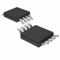
LT1567CMS8#TRPBF Linear Technology, LT1567CMS8#TRPBF Datasheet

LT1567CMS8#TRPBF
Specifications of LT1567CMS8#TRPBF
Available stocks
Related parts for LT1567CMS8#TRPBF
LT1567CMS8#TRPBF Summary of contents
Page 1
... A/D converters. The LT1567 operates from a total power supply voltage of 2.7V to 12V and supports signal-to-noise ratios above 100dB. The LT1567 is available in an 8-lead MSOP package. , LTC, LT and LTM are registered trademarks of Linear Technology Corporation. All other trademarks are the property of their respective owners 0.1µ ...
Page 2
LT1567 ABSOLUTE AXI U RATI GS (Note 1) + – Total Supply Voltage ( ............................ 12.6V Input Current (Note 2) ........................................ ±25mA Operating Temperature Range (Note 3) LT1567C ..............................................–40°C to 85°C LT1567I ...............................................–40°C to ...
Page 3
ELECTRICAL CHARACTERISTICS The ● denotes the specifications that apply over the full operating temperature range (Note 4), otherwise specifications and typical = ±2.5V, R values are 25° PARAMETER OA Input Bias Current DC ...
Page 4
LT1567 W U TYPICAL PERFOR A CE CHARACTERISTICS OA Open-Loop Gain and Phase vs Frequency –10 –20 –30 0 FREQUENCY (MHz) Closed-Loop Gain and Phase of OA and INV vs ...
Page 5
W U TYPICAL PERFOR A CE CHARACTERISTICS Output Impedance vs Frequency 100 = ± 25° –10 V INVERTER –1 V 0.01 0.001 100k 1M 10M 100M ...
Page 6
LT1567 CTIO S OAOUT (Pin 1): Output of the Uncommitted Op Amp (OA). As with most wideband op amps important to avoid connecting heavy capacitive loads (above about 10pF) directly to this output. ...
Page 7
W BLOCK DIAGRA OAOUT OAIN BYPASS – + INV 2 – 3 7pF 150Ω – 4 LT1567 + INVOUT 600Ω 600Ω 6 INVIN DC BIAS 5 1567 BD 1567fa 7 ...
Page 8
LT1567 U U APPLICATIO S I FOR ATIO Functional Description The LT1567 contains two low noise rail-to-rail output, wideband operational amplifiers, one of them connected internally as a unity-gain inverter. These two amplifiers can form a second order multiple feedback ...
Page 9
U U APPLICATIO S I FOR ATIO The simple-to-use spreadsheet requires the user to de- fine the desired corner (or center) frequency, the pass- band gain and a capacitor value for a choice of second or third order Chebyshev or ...
Page 10
LT1567 U U APPLICATIO S I FOR ATIO output from the INV block (Pin 7). These two outputs maintain equal gain and 180º phase shift over a wide frequency range. This feature permits choosing the signal polarity in single ended ...
Page 11
U U APPLICATIO S I FOR ATIO 0.1µ REF Figure 3. A Single Ended to Differential Amplifier LT1567 600Ω 600Ω 2 – – 7pF 150Ω + – ...
Page 12
LT1567 U U APPLICATIO S I FOR ATIO Figure 4 shows an LT1567 single supply differential buffer driving a differential 1st order RC filter. The V is subject to the common mode (DC BIAS) limits in the spec table. Within ...
Page 13
U U APPLICATIO S I FOR ATIO V IN2 R1 V IN1 V REF WITH R3 AND R1 EQUAL, V GAIN FROM ( 604Ω, THEN NOISE ...
Page 14
LT1567 U U APPE DIX: OUTPUT OISE VERTI G A PLIFIER NOISE THEN the voltage noise density in V/√Hz at the inverter’s ON output. V ...
Page 15
... LEAD COPLANARITY (BOTTOM OF LEADS AFTER FORMING) SHALL BE 0.102mm (.004") MAX Information furnished by Linear Technology Corporation is believed to be accurate and reliable. However, no responsibility is assumed for its use. Linear Technology Corporation makes no represen- tation that the interconnection of its circuits as described herein will not infringe on existing patent rights. ...
Page 16
... CUTOFF f /f CLK CUTOFF f /f CLK CUTOFF www.linear.com ● – V OUT OUT – V 0.1µF – 1567 F06a IN = 150kHz (LTC1562) = 300kHz (LTC1562-2) = 256kHz OUT = 64/ 64kHz (LTC1569-6) CUTOFF(MAX) = 32/ 374kHz (LTC1569-7) CUTOFF(MAX) LT 0406 REV A • PRINTED IN USA © LINEAR TECHNOLOGY CORPORATION 2001 1567fa ...


