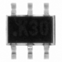
TSH122ICT STMicroelectronics, TSH122ICT Datasheet

TSH122ICT
Specifications of TSH122ICT
Available stocks
Related parts for TSH122ICT
TSH122ICT Summary of contents
Page 1
Ultra low power video buffer/filter with power-down Features ■ Very low consumption: 1.7 mA ■ Ultra low power-down mode typ., 500 nA max. th ■ Internal 6 order reconstruction filter ■ Internal gain Rail-to-rail output ...
Page 2
Absolute maximum ratings and operating conditions 1 Absolute maximum ratings and operating conditions Table 1. Absolute maximum ratings Symbol Supply voltage V CC Maximum input amplitude Storage temperature stg T Maximum junction temperature j R SC70 thermal ...
Page 3
TSH122 2 Electrical characteristics Table +2.5V, +3.3V Symbol Parameter DC performance V Output DC level shift dc I Input bias current ib G Internal voltage gain Power supply rejection ratio PSRR 20 log (ΔV /ΔV ...
Page 4
Electrical characteristics Table +2.5V, +3.3V Symbol Parameter V Low level output voltage OL I Output short circuit current out Noise and distortion eN Total output noise HD Harmonic distortion Enable/power-down Low level on pin-5: TSH122 ...
Page 5
TSH122 Figure 1. Frequency response 10 0 -10 -20 -30 -40 -50 Vcc=3.3V -60 Ω Load=150 -70 Small signal Vicm=0.5V -80 1M 10M Frequency (Hz) Figure 3. Input noise 250 200 150 100 50 0 100 1k 10k Frequency (Hz) ...
Page 6
Electrical characteristics Figure 7. DCshift vs. Vcc 125 124 123 122 121 120 119 118 117 116 115 2.0 2.5 3.0 3.5 Vcc (V) Figure 9. Icc vs. Vcc 4.0 3.5 3.0 2.5 2.0 1.5 1.0 0.5 0 ...
Page 7
TSH122 Figure 13. In/Out switch on/off Vin Vout EN (pin5) Vcc=+3.3V Figure 15. VOL vs. temperature 20.0 17.5 15.0 Vcc=+2.5V 12.5 10.0 Vcc=+3.3V 7.5 5.0 2.5 Ω Load=150 0.0 -40 - Temperature (°C) Figure 17. Bandwidth vs. temperature ...
Page 8
Electrical characteristics Figure 19. Icc vs. temperature 3.0 2.5 Vcc=+3.3V 2.0 1.5 1.0 0.5 no Load 0.0 -40 - Temperature (°C) Figure 21. Output DC shift vs. temperature 200 Vcc=+2.5V and +3.3V 180 Ω Load=150 160 140 120 ...
Page 9
TSH122 3 Application information 3.1 Power supply considerations Correct power supply bypassing is very important for optimizing performance in high-frequency ranges. The bypass capacitors should be placed as close as possible to the IC pins to improve high-frequency bypassing. A ...
Page 10
Application information 3.2 Implementation considerations 3.2.1 Input The DC level shifter optimizes the position of the video signal with no clamping on the output rails. 3.2.2 Filter A reconstruction filter is used to attenuate the DAC’s sampling frequency because it ...
Page 11
TSH122 Figure 26. Schematic diagram with output capacitor Figure 27. Schematic diagram without output capacitor Application information 11/16 ...
Page 12
Application information 3.3 Using the TSH122 to drive a Cvbs signal Figure 28. Details on Cvbs (NTSC color bar 100%) DAC output amplitude DAC output amplitude ~1.3 V ~1.3 V +133 IRE +133 IRE White White +100 IRE +100 IRE ...
Page 13
... JEDEC Standard JESD97. The maximum ratings related to soldering conditions are also marked on the inner box label. ECOPACK is an STMicroelectronics trademark. ECOPACK specifications are available at: www.st.com. Figure 29. SC70-6 (or SOT323-6) package footprint (in millimeters) ...
Page 14
Package information Figure 30. SC70-6 (or SOT323-6) package mechanical data Ref 14/16 Dimensions Millimeters Min Typ Max 0.80 1.10 0 0.10 0.80 1.00 0.15 0.30 0.10 0.18 1.80 ...
Page 15
... TSH122 5 Ordering information Table 4. Order codes Part number TSH122ICT 6 Revision history Table 5. Document revision history Date 04-Aug-2008 Temperature range Package -40°C to +85°C SC70 Revision 1 Initial release. Ordering information Packaging Marking Tape & reel K31 Changes 15/16 ...
Page 16
... Information in this document is provided solely in connection with ST products. STMicroelectronics NV and its subsidiaries (“ST”) reserve the right to make changes, corrections, modifications or improvements, to this document, and the products and services described herein at any time, without notice. All ST products are sold pursuant to ST’s terms and conditions of sale. ...


