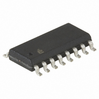
EL4332CSZ Intersil, EL4332CSZ Datasheet

EL4332CSZ
Specifications of EL4332CSZ
Available stocks
Related parts for EL4332CSZ
EL4332CSZ Summary of contents
Page 1
... EL4332CS-T13 EL4332CSZ (Note) EL4332CSZ-T7 (Note) EL4332CSZ-T13 (Note) NOTE: Intersil Pb-free products employ special Pb-free material sets; molding compounds/die attach materials and 100% matte tin plate termination finish, which is compatible with both SnPb and Pb-free soldering operations. Intersil Pb-free products are MSL classified at Pb-free peak reflow temperatures that meet or exceed the Pb-free requirements of IPC/JEDEC J Std-020B ...
Page 2
Absolute Maximum Ratings ( ...
Page 3
AC Electrical Specifications V PARAMETER t Settling Time to 0.1% of Final Value S T Time to Switch Inputs SW OS Overshoot, V OUT I ab 10M Input to Input Isolation at 10MHz SO 100M Input to Input Isolation at ...
Page 4
Typical Performance Curves FIGURE 1. SMALL SIGNAL TRANSIENT RESPONSE FIGURE 3. SWITCHING TO GROUND FROM A LARGE SIGNAL UNCORRELATED SINE WAVE FIGURE 5. SWITCHING TO GROUND FROM A SMALL SIGNAL UNCORRELATED SINE WAVE FIGURE 7. SWITCHING GLITCH (INPUTS AT GROUND) ...
Page 5
Typical Performance Curves FIGURE 9. SWITCHING FROM GROUND TO A FAMILY OF DC LEVELS FIGURE 11. GAIN vs FREQUENCY FIGURE 13. -3dB BW vs SUPPLY VOLTAGE 5 EL4332 (Continued) FIGURE 10. CHANNEL A/B SWITCHING DELAY FIGURE 14. BANDWIDTH vs DIE ...
Page 6
Typical Performance Curves FIGURE 15. FREQUENCY RESPONSE WITH CAPACITIVE LOADS FIGURE 17. A-INPUT TO B–INPUT ISOLATION FIGURE 19. OUTPUT SWING vs SUPPLY VOLTAGE 6 EL4332 (Continued) FIGURE 16. INPUT VOLTAGE NOISE OVER FREQUENCY FIGURE 18. CHANNEL-CHANNEL ISOLATION FIGURE 20. OUTPUT ...
Page 7
Typical Performance Curves FIGURE 21. SLEW RATE vs SUPPLY VOLTAGE FIGURE 23. SUPPLY CURRENT vs SUPPLY VOLTAGE FIGURE 25. POWER DISSIPATION vs AMBIENT TEMPERATURE 7 EL4332 (Continued) FIGURE 22. SLEW RATE vs DIE TEMPERATURE FIGURE 24. POWER DISSIPATION vs AMBIENT ...
Page 8
FIGURE 26. TYPICAL CONNECTION FOR A 2:1 COMPONENT VIDEO MULTIPLEXER Applications Information Figure 26 shows a typical use for the EL4332. The circuit is a component video (R, Y,U,V) multiplexer. Since the gain of the internal amplifiers has ...
Page 9
Logic Inputs The A/B select, logic input, is internally referenced to ground set at 2 diode drops above ground, to give a threshold of about 1.4V (see Figure 27). The PNP input transistor requires that the driving gate ...
Page 10
Expanding the Multiplexer In Figure 29, a 3:1 multiplexer circuit is shown. The expansion to more inputs is very straight forward. Since the EL4332 has a fixed gain of 2, interstage attenuators may be required as shown in Figure 28. ...
Page 11
A Bandwidth Selectable Circuit In Figure 30, a circuit is shown that allows three signals to be either low pass filtered or full bandwidth. FIGURE 30. SWITCHED 50MHz LOW PASS FILTER FOR HIGH/LOW RESOLUTION MONITORS 11 EL4332 This could be ...
Page 12
EL4332 Macromodel * EL4332 Macromodel * Revision A, April 1996 **************************************************************************** *Applications Hints. The EL4332 has two V *pins. The V pins (pins 14 and 15 are internally shorted together in the model, CC *but the ground pins (GND1, GND2, ...
Page 13
R51 105 13 275 R61 106 13 275 R71 1 114 400 R81 114 2 400 R911 117 400 R110 117 2 400 Ediff1 108 0 value {(v(104,103)*v(107))+(v(106,105)*(1-v(107)))} rdiff1 108 *Compensation Section * ga1 0 134 108 ...
Page 14
Poles * ep2 241 0 234 0 1.0 rpa2 241 242 200 cpa2 242 0 0.75 pF rpb2 242 243 200 cpb2 243 0 0. *Output Stage * 250 1.0 mA i022 251 ...
Page 15
... Accordingly, the reader is cautioned to verify that data sheets are current before placing orders. Information furnished by Intersil is believed to be accurate and reliable. However, no responsibility is assumed by Intersil or its subsidiaries for its use; nor for any infringements of patents or other rights of third parties which may result from its use ...


