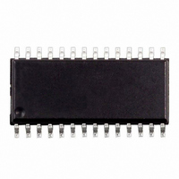
TDA7439DS13TR STMicroelectronics, TDA7439DS13TR Datasheet

TDA7439DS13TR
Specifications of TDA7439DS13TR
Available stocks
Related parts for TDA7439DS13TR
TDA7439DS13TR Summary of contents
Page 1
Features ! Input multiplexer – four stereo inputs – selectable input gain for optimal adaptation to different sources ! Single stereo output ! Treble, mid-range and bass control in 2-dB steps ! Volume control in 1-dB steps ! Two speaker ...
Page 2
Contents Contents 1 Block diagram and pin out . . . . . . . . . . . . . . . . . . . . . . . . . . . . . . . . ...
Page 3
TDA7439DS 1 Block diagram and pin out Figure 1. Block diagram 4 L-IN1 100K 5 L-IN2 100K 6 L-IN3 100K 7 L-IN4 100K 3 R-IN1 100K 2 R-IN2 100K 1 R-IN3 100K 28 R-IN4 100K Figure 2. Pin connections MUXOUTL ...
Page 4
Electrical specifications 2 Electrical specifications Table 2. Absolute maximum ratings Symbol V Operating supply voltage S T Operating ambient temperature amb T Storage temperature range stg Table 3. Thermal data Symbol R Thermal resistance junction-pins th j-pin Table 4. Quick ...
Page 5
TDA7439DS Table 5. Electrical characteristics (continued) Symbol Input stage R Input resistance IN V Clipping level CL S Input separation IN G Minimum input gain in_min G Maximum input gain in_max G Step resolution step Volume control R Volume control ...
Page 6
Electrical specifications Table 5. Electrical characteristics (continued) Symbol Speaker attenuators C Control range range S Step resolution step E A Attenuation set error V DC step DC A Mute attenuation mute Audio outputs V Clipping level CLIP R Output load ...
Page 7
TDA7439DS Figure 3. Test circuit L-IN1 0.47µF L-IN2 0.47µF L-IN3 0.47µF L-IN4 0.47µF R-IN1 0.47µF R-IN2 0.47µF R-IN3 0.47µF R-IN4 0.47µF 5.6nF MUXOUTL TREBLE( 100K 5 100K 6 G VOLUME TREBLE 100K 7 100K 0/30dB 2 I ...
Page 8
Application suggestions 3 Application suggestions The first and the last stages are volume control blocks. The control range -47 dB and mute for the first stage and 0 to -79 dB and mute for the last one. ...
Page 9
TDA7439DS Transposing and solving for the external components we get: = ----------------------------------------- - C1 2 π ⋅ ⋅ ----------------------------- - C2 – --------------------------------------------------------------------- - R2 2 π ⋅ ⋅ 3.1.2 ...
Page 10
Application suggestions Figure 7. Channel separation vs frequency Figure 9. Mid-range filter response Figure 11. Typical tone response 10/23 Figure 8. Bass filter response Figure 10. Treble filter response TDA7439DS ...
Page 11
TDA7439DS bus interface Data transmission from the microprocessor to the TDA7439DS and vice versa takes place through the 2-wire I Pull-up resistors to the positive supply voltage must be used (there are no internal pull-ups). 4.1 ...
Page 12
I C bus interface Figure 12. Timing diagram of the data on the I SCL SDA Figure 13. Timing diagram of the start/stop SCL SDA Start Figure 14. Timing diagram of the acknowledge SCL SDA Start 4.6 Interface protocol ...
Page 13
TDA7439DS bus transmission examples 5.1 No address incrementing The TDA7439DS receives a start condition followed by the correct chip address, then a sub address with the bit (for no address increment), then the ...
Page 14
I C bus addresses and data bus addresses and data 6.1 Chip address byte The TDA7439DS chip address is 0x88. 6.2 Sub-address byte The function is selected by the 4-bit sub address as given in ...
Page 15
TDA7439DS Table 9. Input gain value (sub address 0x1) MSB ...
Page 16
I C bus addresses and data Table 11. Bass gain value (sub address 0x3) MSB ...
Page 17
TDA7439DS Table 13. Treble gain value (sub address 0x5) MSB ...
Page 18
I C bus addresses and data Table 14. Speaker attenuation value (sub address 0x6, 0x7) (continued) MSB 18/ ...
Page 19
TDA7439DS 7 Chip input/output circuits Figure 18. Pin 23 V CREF Figure 20. Pins 100K V REF Figure 22. Pins 11 MOUT(L) MOUT(R) Figure 19. Pins ...
Page 20
Chip input/output circuits Figure 24. Pins 12 BIN(L) BIN(R) Figure 26. Pins 18 TREBLE(L) TREBLE(R) Figure 28. Pin 22 SDA 20/23 Figure 25. Pins 13, 15 20µA 44K BOUT(L) BOUT(R) D96AU428 Figure 27. Pin ...
Page 21
TDA7439DS 8 Package information mm DIM. MIN. TYP. MAX. A 2.65 a1 0.1 0.3 b 0.35 0.49 b1 0.23 0.32 C 0.5 c1 45° (typ.) D 17.7 18 10.65 e 1.27 e3 16.51 F 7.4 7.6 L 0.4 ...
Page 22
Revision history 9 Revision history Table 15. Document revision history Date Jan-2004 Jun-2004 14-Nov-2007 20-Nov-2007 22/23 Revision 1 Initial release 2 Modified presentation Updated titles to Figure 9 3 Minor updates to presentation 4 Updated Figure 23 and TDA7439DS Changes ...
Page 23
... TDA7439DS Information in this document is provided solely in connection with ST products. STMicroelectronics NV and its subsidiaries (“ST”) reserve the right to make changes, corrections, modifications or improvements, to this document, and the products and services described herein at any time, without notice. All ST products are sold pursuant to ST’s terms and conditions of sale. ...


