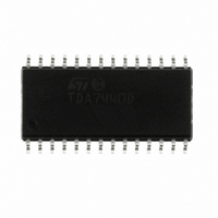
TDA7440D013TR STMicroelectronics, TDA7440D013TR Datasheet

TDA7440D013TR
Specifications of TDA7440D013TR
Available stocks
Related parts for TDA7440D013TR
TDA7440D013TR Summary of contents
Page 1
... R-IN4 INPUT MULTIPLEXER 100K April 2010 Figure 1. Package Table 1. Order Codes TDA7440D013TR Selectable input gain is provided. Control of all the functions is accomplished by serial bus. The AC signal setting is obtained by resistor net- works and switches combined with operational amplifiers. Thanks to the used BIPOLAR/CMOS Technology, ...
Page 2
TDA7440 Figure 3. Pin Connection (Top view) MUXOUTL MUXOUT(R) Table 2. Absolute Maximum Ratings Symbol V Operating Supply Voltage S T Operating Ambient Temperature amb T Storage Temperature Range stg Table 3. Thermal Data Symbol R Thermal Resistance Junction-pins th ...
Page 3
Table 5. Electrical Characteristcs Refer to the test circuit T = 25°C, V amb otherwise specified. Symbol Parameter SUPPLY V Supply Voltage S I Supply Current S SVR Ripple Rejection INPUT STAGE R Input Resistance IN V Clipping Level CL ...
Page 4
TDA7440 Table 5. Electrical Characteristcs (continued) Refer to the test circuit T = 25°C, V amb otherwise specified. Symbol Parameter AUDIO OUTPUTS V Clipping Level CLIP R Output Load Resistance L R Output Impedance Voltage Level DC ...
Page 5
APPLICATION SUGGESTIONS The first and the last stages are volume control blocks. The control range -47dB (mute) for the first one -79dB (mute) for the last one. Both of them have 1dB step resolution. ...
Page 6
TDA7440 Figure 6. THD vs. frequency Figure 7. THD vs. R LOAD Figure 8. Channel separation vs. frequency 6/17 Figure 9. Bass response R = 44kΩ C10 = 100nF (Bout, Bin 5.6kΩ Figure 10. Treble ...
Page 7
I C BUS INTERFACE Data transmission from microprocessor to the TDA7440D and vice versa takes place through the 2 wires BUS interface, consisting of the two lines SDA and SCL (pull-up resistors to positive supply ...
Page 8
TDA7440 5 SOFTWARE SPECIFICATION Interface Protocol The interface protocol comprises: A start condition (S) A chip address byte, containing the TDA7440D A subaddress bytes A sequence of data (N byte + acknowledge) A stop condition (P) CHIP ADDRESS MSB LSB ...
Page 9
POWER ON RESET CONDITION Table 6. INPUT SELECTION INPUT GAIN VOLUME BASS TREBLE SPEAKER 5.3 DATA BYTES Address = 88 HEX (ADDR:OPEN). Table 7. FUNCTION SELECTION: First byte (subaddress) MSB ...
Page 10
TDA7440 5.3 DATA BYTES (continued) Table 10. INPUT GAIN SELECTION MSB GAIN = 0 to 30dB Table 11. VOLUME SELECTION MSB ...
Page 11
DATA BYTES (continued) Table 12. BASS SELECTION MSB Table 13. TREBLE SELECTION MSB LSB ...
Page 12
TDA7440 5.3 DATA BYTES (continued) Table 14. SPEAKER ATTENUATE SELECTION MSB ...
Page 13
Figure 14. PINS CREF Figure 15. PINS: 26 ROUT LOUT 20µA D96AU434 Figure 16. PINS 100K V REF Figure 17. ...
Page 14
TDA7440 Figure 20. PINS: 13 BOUT(L) BOUT(R) Figure 21. PINS: 18 TREBLE(L) TREBLE(R) 50K 6 PACKAGE MECHANICAL DATA In order to meet environmental requirements, ST offers these devices in different grades of ECOPACK packages, ...
Page 15
Figure 24. SO-28 Mechanical Data & Package Dimensions mm DIM. MIN. TYP. MAX. A 2.65 a1 0.1 0.3 b 0.35 0.49 b1 0.23 0.32 C 0.5 c1 45° (typ.) D 17.7 18 10.65 e 1.27 e3 16.51 F ...
Page 16
TDA7440 7 REVISION HISTORY Table 15. Revision History Date Revision January 2004 June 2004 30-Apr-2010 16/17 2 First Issue 3 Modified the style-sheet in compliance with the last revision of the “Corporate Technical Pubblications Design Guide”. 4 Updated title and ...
Page 17
... ST and the ST logo are trademarks or registered trademarks various countries. Information in this document supersedes and replaces all information previously supplied. The ST logo is a registered trademark of STMicroelectronics. All other names are the property of their respective owners. Australia - Belgium - Brazil - Canada - China - Czech Republic - Finland - France - Germany - Hong Kong - India - Israel ...


