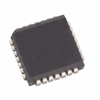
DS2165Q+ Maxim Integrated Products, DS2165Q+ Datasheet

DS2165Q+
Specifications of DS2165Q+
Related parts for DS2165Q+
DS2165Q+ Summary of contents
Page 1
FEATURES § Compresses/expands 64kbps PCM voice to/from either 32kbps, 24kbps, or 16kbps § Dual fully independent channel architecture; device can be programmed to perform either: - two expansions - two compressions - one expansion and one compression § Interconnects ...
Page 2
OVERVIEW The DS2165Q contains three major functional blocks: a high performance (10 MIPS) DSP engine, two independent PCM interfaces (X and Y) that connect directly to serial time-division-multiplexed (TDM) backplanes, and a serial port that can configure the device on-the-fly ...
Page 3
CONTROL REGISTER The control register establishes idle, algorithm reset, bypass, data format, and channel coding for the selected channel. The X-side and Y-side PCM interfaces can be independently disabled (output tri-stated) by IPD. When IPD is set for both channels, ...
Page 4
Figure 1. BLOCK DIAGRAM Figure 2. SERIAL PORT WRITE Note: A 2-byte write is shown. The bypass feature is enabled when BYP is set and IPD is cleared. During bypass, no expansion or compression occurs. Bypass operates on bytewide (8 ...
Page 5
Figure 3. ADDRESS/COMMAND BYTE (MSB) — SYMBOL POSITION — ACB.7 ACB ACB.5 A4 ACB.4 A3 ACB.3 A2 ACB.2 A1 ACB.1 A0 ACB.0 Figure 4. CONTROL REGISTER (MSB) AS0 AS1 SYMBOL POSITION AS0 CR.7 AS1 CR.6 ...
Page 6
Table 2. ALGORITHM SELECT BITS ALGORITHM SELECTED 64kbps to/from 32kbps 64kbps to/from 24kbps 64kbps to/from 16kbps Figure 5. INPUT TIME SLOT REGISTER (MSB) — —- SYMBOL POSITION — ITR.7 — ITR.6 D5 ITR.5 D4 ITR.4 D3 ITR.3 D2 ITR.2 D1 ...
Page 7
TIME SLOT ASSIGNMENT/ORGANIZATION On-board counters establish when PCM and ADPCM I/O occur. The counters are programmed by the time slot registers. Time slot size (number of bits wide) is determined by the state of CP/ of time slots available is ...
Page 8
Figure 9. A-LAW PCM INTERFACE Figure 10. A-LAW ADPCM INTERFACE DS2165Q ...
Page 9
HARDWARE MODE The hardware mode is intended for applications that do not have an external controller available or do not require the extended features offered by the serial port. Connecting the SPS pin to V port, clears all internal register ...
Page 10
Table 4. ALGORITHM SELECT FOR HARDWARE MODE ALGORITHM 64kbps to/from 32kbps Connect both A1 and Hold A1 and A4 low during a hardware reset; take both A1 and A4 high after the 64kpbs to/from 24kbps has returned ...
Page 11
PCM AND ADPCM INPUT/OUTPUT Since the organization of the input and output time slots on the DS2165Q does not depend on the algorithm selected, it always assumes that PCM input and output are in 8-bit bytes and that ADPCM input ...
Page 12
TIME SLOT RESTRICTIONS Under certain conditions, the DS2165Q does contain some restrictions on the output time slots that are available. These restrictions are covered in detail in a separate application note. No restrictions occur if the DS2165Q is operated in ...
Page 13
ABSOLUTE MAXIMUM RATINGS* Voltage Range on Any Pin Relative to Ground Operating Temperature Range Storage Temperature Range Soldering Temperature Range *This is a stress rating only and functional operation of the device at these or any other conditions beyond those ...
Page 14
PCM INTERFACE, AC ELECTRICAL CHARACTERISTICS ( ±10 PARAMETER CLKX, CLKY Period CLKX, CLKY Pulse Width CLKX, CLKY Rise Fall Times Hold Time from CLKX, CLKY to FSX, FSY Setup Time from FSX, FSY High to CLKX, ...
Page 15
SERIAL PORT, AC ELECTRICAL CHARACTERISTICS ( ±10 PARAMETER SDI to SCLK Setup SCLK to SDI Hold SCLK Low Time SCLK High Time SCLK Rise and Fall Time CS to SCLK Setup SCLK to Hold CS CS ...
Page 16
Figure 13. PCM INTERFACE AC TIMING DIAGRAM Figure 14. MASTER CLOCK/RESET AC TIMING DIAGRAM Figure 15. SERIAL PORT AC TIMING DIAGRAM Note: SCLK can be either high or low when CS is taken low DS2165Q ...
Page 17
PLCC INCHES DIM MIN MAX A 0.165 0.180 A1 0.090 0.120 A2 0.020 — B 0.026 0.033 B1 0.013 0.021 C 0.009 0.012 D 0.485 0.495 D1 0.450 0.456 D2 0.390 0.430 E 0.485 0.495 E1 0.450 0.456 E2 ...


