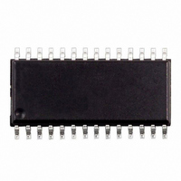
TDA7440D STMicroelectronics, TDA7440D Datasheet

TDA7440D
Specifications of TDA7440D
Available stocks
Related parts for TDA7440D
TDA7440D Summary of contents
Page 1
... TWO INDEPENDENT SPEAKER CONTROL IN 1.0dB STEPS FOR BALANCE FACILITY – INDEPENDENT MUTE FUNCTION ALL FUNCTION ARE PROGRAMMABLE VIA SERIAL BUS 2 DESCRIPTION The TDA7440D is a volume tone (bass and treble) balance (Left/Right) processor for quality audio applications in Hi-Fi systems. Figure 2. Block Diagram 4 L-IN1 100K ...
Page 2
TDA7440 Figure 3. Pin Connection (Top view) MUXOUTL MUXOUT(R) Table 2. Absolute Maximum Ratings Symbol V Operating Supply Voltage S T Operating Ambient Temperature amb T Storage Temperature Range stg Table 3. Thermal Data Symbol R Thermal Resistance Junction-pins th ...
Page 3
Table 5. Electrical Characteristcs Refer to the test circuit T = 25°C, V amb otherwise specified. Symbol Parameter SUPPLY V Supply Voltage S I Supply Current S SVR Ripple Rejection INPUT STAGE R Input Resistance IN V Clipping Level CL ...
Page 4
TDA7440 Table 5. Electrical Characteristcs (continued) Refer to the test circuit T = 25°C, V amb otherwise specified. Symbol Parameter AUDIO OUTPUTS V Clipping Level CLIP R Output Load Resistance L R Output Impedance Voltage Level DC ...
Page 5
... Both of them have 1dB step resolution. The very high resolution allows the implementation of systems free from any noisy acoustical effect. The TDA7440D audioprocessor provides 3 bands tones control. 3.1 Bass Stage Several filter types can be implemented, connecting external components to the Bass IN and OUT pins. ...
Page 6
TDA7440 Figure 6. THD vs. frequency Figure 7. THD vs. R LOAD Figure 8. Channel separation vs. frequency 6/17 Figure 9. Bass response R = 44kΩ C10 = 100nF (Bout, Bin 5.6kΩ Figure 10. Treble ...
Page 7
... I C BUS INTERFACE Data transmission from microprocessor to the TDA7440D and vice versa takes place through the 2 wires BUS interface, consisting of the two lines SDA and SCL (pull-up resistors to positive supply voltage must be connected). 4.1 Data Validity As shown in fig. 11, the data on the SDA line must be stable during the high period of the clock. The HIGH and LOW state of the data line can only change when the clock signal on the SCL line is LOW ...
Page 8
... ACK = Acknowledge S = Start P = Stop A = Address B = Auto Increment 5.1 EXAMPLES 5.1.1 No Incremental Bus The TDA7440D receives a start condition, the correct chip address, a subaddress with the (no in- cremental bus), N-datas (all these data concern the subaddress selected), a stop condition. CHIP ADDRESS MSB LSB S 1 ...
Page 9
POWER ON RESET CONDITION Table 6. INPUT SELECTION INPUT GAIN VOLUME BASS TREBLE SPEAKER 5.3 DATA BYTES Address = 88 HEX (ADDR:OPEN). Table 7. FUNCTION SELECTION: First byte (subaddress) MSB ...
Page 10
TDA7440 5.3 DATA BYTES (continued) Table 10. INPUT GAIN SELECTION MSB GAIN = 0 to 30dB Table 11. VOLUME SELECTION MSB ...
Page 11
DATA BYTES (continued) Table 12. BASS SELECTION MSB Table 13. TREBLE SELECTION MSB LSB ...
Page 12
TDA7440 5.3 DATA BYTES (continued) Table 14. SPEAKER ATTENUATE SELECTION MSB ...
Page 13
Figure 14. PINS CREF Figure 15. PINS: 26 ROUT LOUT 20µA D96AU434 Figure 16. PINS 100K V REF Figure 17. ...
Page 14
TDA7440 Figure 20. PINS: 13 BOUT(L) BOUT(R) Figure 21. PINS: 18 TREBLE(L) TREBLE(R) 50K 6 PACKAGE MECHANICAL DATA In order to meet environmental requirements, ST offers these devices in different grades of ECOPACK packages, ...
Page 15
Figure 24. SO-28 Mechanical Data & Package Dimensions mm DIM. MIN. TYP. MAX. A 2.65 a1 0.1 0.3 b 0.35 0.49 b1 0.23 0.32 C 0.5 c1 45° (typ.) D 17.7 18 10.65 e 1.27 e3 16.51 F ...
Page 16
TDA7440 7 REVISION HISTORY Table 15. Revision History Date Revision January 2004 June 2004 30-Apr-2010 16/17 2 First Issue 3 Modified the style-sheet in compliance with the last revision of the “Corporate Technical Pubblications Design Guide”. 4 Updated title and ...
Page 17
... ST and the ST logo are trademarks or registered trademarks various countries. Information in this document supersedes and replaces all information previously supplied. The ST logo is a registered trademark of STMicroelectronics. All other names are the property of their respective owners. Australia - Belgium - Brazil - Canada - China - Czech Republic - Finland - France - Germany - Hong Kong - India - Israel ...


