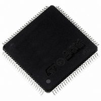
TDA7500A STMicroelectronics, TDA7500A Datasheet - Page 31

TDA7500A
Manufacturer Part Number
TDA7500A
Description
IC PROCESSOR AM/FM DGTL 100-TQFP
Manufacturer
STMicroelectronics
Type
Audio Processorr
Datasheet
1.TDA7500ATR.pdf
(40 pages)
Specifications of TDA7500A
Applications
Audio Systems
Mounting Type
Surface Mount
Package / Case
100-TQFP Exposed Pad, 100-eTQFP, 100-HTQFP, 100-VQFP
Lead Free Status / RoHS Status
Lead free / RoHS Compliant
Available stocks
Company
Part Number
Manufacturer
Quantity
Price
Company:
Part Number:
TDA7500ATR
Manufacturer:
STMicroelectronics
Quantity:
10 000
Part Number:
TDA7500ATR
Manufacturer:
ST
Quantity:
20 000
Figure 17. DSP1 and DSP0 Memory Spaces
Serial Audio Interface (SAI)
The SAI is used to deliver digital audio to the DSPs from an external source. Once processed by the DSPs, it
can be returned through this interface either sent to the DAC for D/A conversion. The features of the SAI are
listed below.
XCHG Interface (DSP to DSP Exchange Interface)
The Exchange Interface peripheral provides bidirectional communication between DSP0 and DSP1. Both 24 bit
word data and four bit Flag data can be exchanged. A FIFO is utilized for received data. It minimizes the number
of times an Exchange Interrupt Service Routine would have to be called if multi-word blocks of data were to be
received. The Transmit FIFO is in effect the Receive FIFO of the other DSP and is written directly by the trans-
mitting DSP. The features of the XCHG are listed below.
DRAM/SRAM Interface (EMI)
The External DRAM/SRAM Interface is viewed as a memory mapped peripheral. Data transfers are performed
by moving data into/from data registers and the control is exercised by polling status flags in the control/status
register or by servicing interrupts. An external memory write is executed by writing data into the EMI Data Write
Register. An external memory read operation is executed by either writing to the offset register or reading the
EMI Data Read Register, depending on the configuration.
3 Synchronized Stereo Data Transmission Lines
3 Synchronized Stereo Data Reception Lines
Master and Slave operating mode: clock lines can be both master and slave.
Receive and Transmit Data Registers have two locations to hold left and right data.
10 Word XCHG Receive FIFO on both DSPs
Four Flags for each XCHG for DSP to DSP signaling
Condition flags can optionally trigger interrupts on both DSPs
$FFFF
$0000
$01FF
$0200
Boot-Space
Not Accessible
Boot-ROM
$FFFF
$15FF
$1600
Not Accessible Not Accessible
P-Space
$FFFF
P-RAM
$0400
$03FF
$FFC0
$FFBF
DSP0
X-Peripherals
X-Space
X-RAM
Not Accessible
Y-Space
Y-RAM
$FFFF
$0000
$00FF
$0100
Boot-Space
Not Accessible
Boot-ROM
$FFFF
$0800
$07FF
Not Accessible Not Accessible
P-Space
$FFFF
P-RAM
$0400
$03FF
$FFC0
$FFBF
DSP1
X-Space
X-Peripherals
X-RAM
Not Accessible
Y-Space
Y-RAM
TDA7500A
31/40


