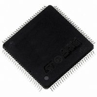
TDA7500A STMicroelectronics, TDA7500A Datasheet - Page 32

TDA7500A
Manufacturer Part Number
TDA7500A
Description
IC PROCESSOR AM/FM DGTL 100-TQFP
Manufacturer
STMicroelectronics
Type
Audio Processorr
Datasheet
1.TDA7500ATR.pdf
(40 pages)
Specifications of TDA7500A
Applications
Audio Systems
Mounting Type
Surface Mount
Package / Case
100-TQFP Exposed Pad, 100-eTQFP, 100-HTQFP, 100-VQFP
Lead Free Status / RoHS Status
Lead free / RoHS Compliant
Available stocks
Company
Part Number
Manufacturer
Quantity
Price
Company:
Part Number:
TDA7500ATR
Manufacturer:
STMicroelectronics
Quantity:
10 000
Part Number:
TDA7500ATR
Manufacturer:
ST
Quantity:
20 000
TDA7500A
The features of the EMI are listed below.
Debug Interface
A dedicated Debug Port is available for each DSP Cores. The debug logic is contained in the core design of the
DSP. The features of the Debug Port are listed below:
Serial Peripheral Interface
The DSP core requires a serial interface to receive commands and data over the LAN. During an SPI transfer,
data is transmitted and received simultaneously. A serial clock line synchronizes shifting and sampling of the
information on the two serial data lines. A slave select line allows individual selection of a slave SPI device.
When an SPI transfer occurs an 8-bit word is shifted out one data pin while another 8-bit character is simulta-
neously shifted in a second data pin.The central element in the SPI system is the shift register and the read data
buffer. The system is single buffered in the transfer direction and double buffered in the receive direction.
I
The inter Integrated Circuit bus is a single bidirectional two-wire bus used for efficient inter IC control. All I
bus compatible devices incorporate an on-chip interface which allows them communicate directly with each oth-
er via the I
Every component hooked up to the I2C bus has its own unique address whether it is a CPU, memory or some
other complex function chip. Each of these chips can act as a receiver and /or transmitter on its functionality.
General Purpose Input/Output
The DSP requires a set of external general purpose input/output lines, and a reset line. These signals are used
by external devices to signal events to the DSP. The GPIO lines are implemented as DSP 's peripherals. The
GPIO lines are grouped in Port A which is connected to DSP 0, and Port B, which is connected to DSP1.
RDS
The RDS block is an hardware cell able to deliver the RDS frames through a dedicated serial interface. RDS
quality signalis also available. This block needs to be initialised at reset by the DSP, after that it works in back-
ground and does not need any further DSP support. RDS is made of 57kHz filter, demodulator and decoder.
32/40
2
C Interface
Data bus width fixed at 4 bits for DRAM and 8 bits for SRAM
Data word length 16 or 24 bits for DRAM
Data word length 8 or 16 or 24 bits for SRAM
DRAM address lines means 2
Refresh rate for DRAM can be chosen among eight divider factor
SRAM relative addressing mode; 2
Four SRAM Timing choices
Two Read Offset Registers
Breakpoint Logic
Trace Logic
Single stepping
Instruction Injection
Program Disassembly
2
C bus.
26
= 256MB addressable DRAM
22
= 4MB addressable SRAM
2
C


