LM1894MX/NOPB National Semiconductor, LM1894MX/NOPB Datasheet - Page 3
LM1894MX/NOPB
Manufacturer Part Number
LM1894MX/NOPB
Description
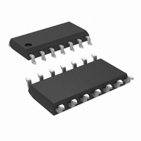
IC NOISE REDUCT SYS DYNAM 14SOIC
Manufacturer
National Semiconductor
Type
Dynamic Noise Reductionr
Datasheet
1.LM1894MXNOPB.pdf
(12 pages)
Specifications of LM1894MX/NOPB
Applications
Automotive Systems, Players, TV
Mounting Type
Surface Mount
Package / Case
14-SOIC (3.9mm Width), 14-SOL
For Use With
LM1894MTBD - BOARD EVALUATION LM1894
Lead Free Status / RoHS Status
Lead free / RoHS Compliant
Other names
*LM1894MX
*LM1894MX/NOPB
LM1894MX
*LM1894MX/NOPB
LM1894MX
Available stocks
Company
Part Number
Manufacturer
Quantity
Price
Company:

Part Number:
LM1894MX/NOPB
Manufacturer:
MS
Quantity:
6 218


Gain Amplifier Input Impedance
Peak Detector Input Impedance
Voltage Gain
Attack Time
Decay Time
DC Voltage Range
Electrical Characteristics
V
Voltage Gain
Note 2: For operation in ambient temperature above 25˚C, the device must be derated based on a 150˚C maximum junction temperature and a thermal resistance
of 1) 80˚C/W junction to ambient for the dual-in-line package, 2) 105˚C/W junction to ambient for the small outline package, and 3) 150˚C/W junction to ambient for
the TSSOP package.
Note 3: To force the DNR system into maximum bandwidth, DC ground the input to the peak detector, pin 9. A negative temperature coefficient of −0.5%/˚C on the
bandwidth, reduces the maximum bandwidth at increased ambient temperature or higher package dissipation. AC ground pin 9 or pin 6 to select minimum
bandwidth. To change minimum and maximum bandwidth, see Appliction Hints.
Note 4: The maximum noise reduction CCIR/ARM weighted is about 14 dB. This is accomplished by changing the bandwidth from maximum to minimum. In actual
operation, minimum bandwidth is not selected, a nominal minimum bandwidth of about 2 kHz gives −10 dB of noise reduction. See Application Hints.
Note 5: The CCIR/ARM weighted noise is measured with a 40 dB gain amplifier between the DNR system and the CCIR weighting filter; it is then input referred.
Note 6: Measured using the Rhode-Schwartz psophometer.
Note 7: Pin 10 is DC forced half way between the maximum bandwidth DC level and minimum bandwidth DC level. An AC 1 kHz signal is then applied to pin 10.
Its peak-to-peak amplitude is V
S
= 8V, T
A
= 25˚C, V
Parameter
IN
DC
= 300 mV at 1 kHz, circuit shown in Figure 1 unless otherwise specified
(max BW) − V
DC
(min BW).
Pin 6
Pin 6 to Pin 8
Pin 9
Pin 9 to Pin 10
Measured to 90% of Final Value
with 10 kHz Tone Burst
Measured to 90% of Final Value
with 10 kHz Tone Burst
Minimum Bandwidth to Maximum
Bandwidth
(Continued)
Conditions
3
21.5
Min
560
300
1.1
24
30
45
Typ
700
500
30
24
33
60
Max
26.5
840
700
3.8
39
36
75
www.national.com
Units
V/V
V/V
kΩ
ms
µs
Ω
V
Related parts for LM1894MX/NOPB
Image
Part Number
Description
Manufacturer
Datasheet
Request
R

Part Number:
Description:
Manufacturer:
National Semiconductor
Datasheet:
Part Number:
Description:
Manufacturer:
National Semiconductor
Datasheet:

Part Number:
Description:
Dynamic Noise Reduction System DNR
Manufacturer:
National Semiconductor
Datasheet:

Part Number:
Description:
IC DYNAM NOISE REDUCT SYS 14SOIC
Manufacturer:
National Semiconductor
Datasheet:
Part Number:
Description:
National Semiconductor [8-Bit D/A Converter]
Manufacturer:
National Semiconductor
Datasheet:
Part Number:
Description:
National Semiconductor [Media Coprocessor]
Manufacturer:
National Semiconductor
Datasheet:
Part Number:
Description:
Digitally Controlled Tone and Volume Circuit with Stereo Audio Power Amplifier, Microphone Preamp Stage and National 3D Sound
Manufacturer:
National Semiconductor
Datasheet:
Part Number:
Description:
Digitally Controlled Tone and Volume Circuit with Stereo Audio Power Amplifier, Microphone Preamp Stage and National 3D Sound
Manufacturer:
National Semiconductor
Datasheet:
Part Number:
Description:
AC97 Rev 2 Codec with Sample Rate Conversion and National 3D Sound
Manufacturer:
National Semiconductor
Part Number:
Description:
Manufacturer:
National Semiconductor
Datasheet:
Part Number:
Description:
Manufacturer:
National Semiconductor
Datasheet:
Part Number:
Description:
General Purpose, Low Voltage, Low Power, Rail-to-Rail Output Operational Amplifiers
Manufacturer:
National Semiconductor
Datasheet:
Part Number:
Description:
8-bit 20 MSPS flash A/D converter.
Manufacturer:
National Semiconductor
Datasheet:
Part Number:
Description:
Low Noise Quad Operational Amplifier
Manufacturer:
National Semiconductor
Datasheet: