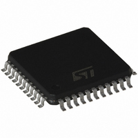
TDA7502 STMicroelectronics, TDA7502 Datasheet - Page 19

TDA7502
Manufacturer Part Number
TDA7502
Description
IC DSP IN-CAR REMOTE AMP 44-LQFP
Manufacturer
STMicroelectronics
Type
Audio Processorr
Datasheet
1.TDA7502.pdf
(25 pages)
Specifications of TDA7502
Applications
Automotive Systems
Mounting Type
Surface Mount
Package / Case
44-LQFP
Device Core Size
24b
Format
Fixed Point
Clock Freq (max)
50MHz
Mips
50
Device Input Clock Speed
50MHz
Ram Size
6KB
Operating Supply Voltage (typ)
3.3V
Operating Supply Voltage (min)
3.15V
Operating Supply Voltage (max)
3.45V
Operating Temp Range
-40C to 125C
Operating Temperature Classification
Automotive
Mounting
Surface Mount
Pin Count
44
Package Type
LQFP
Lead Free Status / RoHS Status
Lead free / RoHS Compliant
Available stocks
Company
Part Number
Manufacturer
Quantity
Price
Company:
Part Number:
TDA7502-013TR
Manufacturer:
RCD
Quantity:
6 639
TDA7502
6.3.5
6.3.6
6.3.7
Essentially this consists of a routine that is called when the DSP comes out of reset. There
are four different boot modes supported by the boot ROM. The first mode loads the
application program via SPI interface where Casper’s SPI is in master mode. The second
boot mode enables the debug port and waits. The third and fourth modes load the
application program via the I
mode and the other in master mode. Which boot mode to enter is configured by sampling
the states of the GPIO4 and GPIO3 pins at reset as shown in the table below.
Table 15.
Serial audio interface (SAI)
The SAI is used to deliver digital audio to the DSPs from an external source. Once
processed by the DSPs, it can be returned through this interface. The features of the SAI
are listed below.
●
●
●
●
●
Serial peripheral interface
A serial interface allows to receive commands and data over the LAN. During an SPI
transfer, data is transmitted and received simultaneously. Both master and slave modes are
supported.
In master mode the SPI supports combination of CPOL =0/1 and CPHA =0 only, while in
slave mode all the 4 possible combinations of CPOL and CPHA are supported. See
9.
A serial clock line synchronizes shifting and sampling of the information on the two serial
data lines. A slave select line allows individual selection of a slave SPI device.
When an SPI transfer occurs an 8-bit word is shifted out one data pin while another 8-bit
character is simultaneously shifted in a second data pin.The central element in the SPI
system is the shift register and the read data buffer. The system is single buffered in the
transfer direction and double buffered in the receive direction.
I
The inter integrated circuit bus is a single bidirectional two-wire bus used for efficient inter IC
control. All I
communicate directly with each other via the I
2
C interface
0-SPI Master
2-I
Three synchronized stereo data transmission lines
Three synchronized stereo data reception lines
Master/Slave operating modes
Transmit and receive interrupt logic triggers on left/right data pairs
Receive and transmit data registers have two locations to hold left and right data.
3-I
1-Debug
2
Modes
2
C Master
C Slave
2
Casper IC boot modes
C bus compatible devices incorporate an on-chip interface which allows them
load PRAM, XRAM and YRAM from SPI
enable Debug Port
load PRAM, XRAM and YRAM from I
oad PRAM, XRAM and YRAM from I
2
C interface, one with Casper’s I
Description
2
C bus.
2
2
C
C
2
C Interface configured in slave
GPIO3
Functional description
0
0
1
1
GPIO4
0
1
0
1
Figure
19/25


