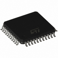
TDA7502 STMicroelectronics, TDA7502 Datasheet - Page 6

TDA7502
Manufacturer Part Number
TDA7502
Description
IC DSP IN-CAR REMOTE AMP 44-LQFP
Manufacturer
STMicroelectronics
Type
Audio Processorr
Datasheet
1.TDA7502.pdf
(25 pages)
Specifications of TDA7502
Applications
Automotive Systems
Mounting Type
Surface Mount
Package / Case
44-LQFP
Device Core Size
24b
Format
Fixed Point
Clock Freq (max)
50MHz
Mips
50
Device Input Clock Speed
50MHz
Ram Size
6KB
Operating Supply Voltage (typ)
3.3V
Operating Supply Voltage (min)
3.15V
Operating Supply Voltage (max)
3.45V
Operating Temp Range
-40C to 125C
Operating Temperature Classification
Automotive
Mounting
Surface Mount
Pin Count
44
Package Type
LQFP
Lead Free Status / RoHS Status
Lead free / RoHS Compliant
Available stocks
Company
Part Number
Manufacturer
Quantity
Price
Company:
Part Number:
TDA7502-013TR
Manufacturer:
RCD
Quantity:
6 639
Block diagram and PIN description
6/25
Table 1.
10
11
12
13
14
15
16
17
18
19
20
21
22
N.
1
2
3
4
5
6
7
8
9
DBOUT/GPIO2
DBCK/GPIO0
DBIN/GPIO1
SCANEN
CLKOUT
TESTEN
DBRQN
RESET
XTO
PGND
Name
GND1
GND2
PVCC
XTI
GND3
VDD1
VDD2
VDD3
SDI0
SDI1
SDI2
Pin description
INT
(1)
(1)
Type
I/O
I/O
I/O
I/O
I/O
G
O
G
O
G
P
P
P
I
I
I
I
I
I
I
I
I
status
Reset
High
–
–
–
–
–
–
–
–
–
–
–
–
–
–
–
–
–
I
I
I
I
Core ground.
External interrupt line (Input/Output). When this line is
asserted low, the DSP may be interrupted. Acts as IRQA
line of DSP core.
SCAN enable when active with TESTEN also active,
controls theshifting of the internal scan chains.
Test enable when active, puts the chip into test mode and
muxes the XTI clock to all flip-flops. When SCANEN is also
active, the scan chain shifting
Debug port request Input. A means of entering the Debug
mode of operation.
The serial data output for the Debug port. Can also be
used as a GPIO.
Core ground.
Debug port Bit Clock/Chip status 1. The serial clock for the
Debug Port is provided when an input. When an output,
provides information about the chip status. Can also be
used as GPIO
Debug port Serial Input/Chip status 0. The serial data
input for the Debug Port is provided when an input. When
an output, provides information about the chip status. Can
also be used as GPIO.
PLL clock ground Input. Ground connection for oscillator
circuit.
PLL clock power supply. Positive supply for PLL clock
oscillator.
Crystal oscillator output. Crystal oscillator output drive.
Crystal oscillator input. External clock input or crystal
connection.
System reset. A logic low level applied to RESET input
initializes DSPs. During debug mode if this pin is pulled
low in while the DBRQN line is pulled low then the DSP
pointed to by the DBSEL pin will be reset.
3.3V core supply.
3.3V core supply.
Output clock.
3.3V supply.
Ground.
SDI0 is a stereo digital audio data input pin channel 0.
SDI1 is a stereo digital audio data input pin channel 1.
SDI2 is a stereo digital audio data input pin channel 2.
Function
TDA7502


