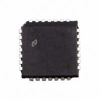
LMC835V National Semiconductor, LMC835V Datasheet - Page 14

LMC835V
Manufacturer Part Number
LMC835V
Description
IC EQUALIZER 7-BAND STERO 28PLCC
Manufacturer
National Semiconductor
Type
Equalizerr
Datasheet
1.LMC835N.pdf
(18 pages)
Specifications of LMC835V
Applications
Receiver
Mounting Type
Through Hole
Package / Case
*
Lead Free Status / RoHS Status
Contains lead / RoHS non-compliant
Other names
*LMC835V
Available stocks
Company
Part Number
Manufacturer
Quantity
Price
Part Number:
LMC835V
Manufacturer:
NS/国半
Quantity:
20 000
ure 15 The gain error is only 0 2 dB and Q error is only 5%
Typical Applications
Application Hints
SWITCHING NOISE
The LMC835 uses CMOS analog switches that have small
leakages (less than 50 nA) When a band is selected for flat
gain all the switches in that band are open and the resona-
tor circuit is not connected to the LMC835 resistor network
It is only in the flat mode that the small leakage currents can
cause problems The input to the resonator circuit is usually
a capacitor and the leakage currents will slowly charge up
this capacitor to a large voltage if there is no resistive path
to limit it When the band is set to any value other than flat
the charge on the capacitor will be discharged by the resis-
tor network and there will be a transient at the output To
limit the size of this transient R
HOW TO AVOID SWITCHING NOISE DUE TO LEAKAGE
CURRENT (Refer to Figures 7 and 8 )
To avoid switching noise due to leakage currents when
changing the gain it is recommended to put R
k
24 each The resistor limits the voltage that the capacitor
can charge to with minimal effects on the equalization The
frequency response change due to R
at 12 dB boost or cut
CODE
335F
335D
335B
3F
05
22
4F
05
07
05
4F
05
07
32
4F
4E
43
48
80
HEX
3C
3D
3E
3F
between Pin 3 and Pin 5 11 each Pin 26 and Pin 12
ADDRESS
RAM
LABEL
LMC835
SEND
DATA
DATA
DATA
DATA
Sample Subroutine Program for Figure 14 LMC835-COP404L CPU Interface
LEAK
MNEMONICS
LBI
LD
SC
OGI
XAS
LD
XDS
LD
XAS
LD
XDS
RC
XAS
OGJ
OGI
CBA
AISC
RET
JP
(Continued)
GAIN DATA D4 D7
GAIN DATA D0 D3
BAND DATA D4 D7
BAND DATA D0 D3
LEAK
is necessary
COMMENTS
are shown in Fig-
3F
13
11
3
SEND
LEAK
e
100
14
POINT TO RAMADDRESS 3F
RAMDATA TO A
SET PORT G 1111 OPEN THE AND GATES
SWAP A AND SIO CLOCK START
RAMDATA TO A MAKE SURE A
SWAP A AND RAMDATA RAMADDRESS RAMADDRESS 1
RAMDATA TO A
SWAP A AND SIO
RAMDATA TO A MAKE SURE A NEWDATA
SWAP A AND RAMDATA RAMADDRESS RAMADDRESS 1
RESET CARRY
SWAP A AND SIO CLOCK STOP
SET PORT G 1101 MAKE STROBE LOW
SET PORT G 1011 MAKE STROBE HIGH CLOSE THE
BD TO A
RAMADDRESS
SET CARRY
ure 2 the data groups are shifted in D0 first Data is loaded
SIMPLE WORD GENERATOR (Figure 6)
Circuit operation revolves around an MM74HC165 parallel-
in serial-out shift register Data bits D0 through D7 are ap-
plied to the parallel of the MM74HC165 from 8 toggle
switches The bits are shifted out to the DATA input of the
LMC835 in sync with the clock When all data bits have
been loaded CLOCK is inhibited and a STROBE pulse is
generated this sequence is initiated by a START pulse
LMC835-COP404L CPU INTERFACE (Refer to Figure 14 )
The diagram shows AND gates between the COP and the
LMC835 These permit G2 to inhibit the CLOCK and DATA
lines (SK and SO) during a STROBE (G1) pulse This func-
tion may also be implemented in software As shown in Fig-
on positive clock edges
POWER SUPPLIES
These applications show LM317 337 regulators for the
5 mA max 1k series dropping resistors from the
amp supply and a pair of 7 5V zeners and bypass caps will
also suffice
g
7 5V supplies for the LMC835 Since the latter draws only
k
3C THEN RETURN
COMMENTS
DATA
GATES
g
15V op


