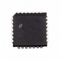
LMC835V National Semiconductor, LMC835V Datasheet - Page 3

LMC835V
Manufacturer Part Number
LMC835V
Description
IC EQUALIZER 7-BAND STERO 28PLCC
Manufacturer
National Semiconductor
Type
Equalizerr
Datasheet
1.LMC835N.pdf
(18 pages)
Specifications of LMC835V
Applications
Receiver
Mounting Type
Through Hole
Package / Case
*
Lead Free Status / RoHS Status
Contains lead / RoHS non-compliant
Other names
*LMC835V
Available stocks
Company
Part Number
Manufacturer
Quantity
Price
Part Number:
LMC835V
Manufacturer:
NS/国半
Quantity:
20 000
LOGIC SECTION
Symbol
I
I
I
I
V
V
f
t
t
t
t
I
C
DDL
SSL
DDH
SSH
o
w(STB)
setup
hold
cs
IN
Absolute Maximum Ratings
If Military Aerospace specified devices are required
please contact the National Semiconductor Sales
Office Distributors for availability and specifications
Supply Voltage V
Allowable Input Voltage (Note 1)
Storage Temperature T
Lead Temperature (Soldering 10 sec) N Pkg
Lead Temperature V Pkg
Electrical Characteristics
Note 1 Pins 2 3 and 26 have a maximum input voltage range of
Note 2 Bold numbers apply at temperature extremes All other numbers apply at T
circuit Figures 3 and 4
Note 3 Guaranteed and 100% production tested
Note 4 Guaranteed (but not 100% production tested) over the operating temperature range These limits are not used to calculate outgoing quality levels
Timing Diagram
IH
IL
IN
Vapor Phase (60 sec)
Infrared (15 sec)
Supply Current
High-Level Input Voltage
Low-Level Input Voltage
Clock Frequency
Width of STB Input
Data Setup Time
Data Hold Time
Delay from Rising Edge of CLOCK
to STB
Input Current
Input Capacitance
Note To change the gain of the presently selected band it is not necessary to send DATA 1 (Band Selection) each time
DD
b
Parameter
V
stg
SS
b
(Note 2) V
60 C to
to V
Pins 14 15 16 are 0V
Pins 14 15 16 are 0V
Pins 14 15 16 are 5V
Pins 14 15 16 are 5V
See Figure 1
See Figure 1
See Figure 1
See Figure 1
V
DD
SS
Pins 14 15 16
Pins 14 15 16
Pin 14
Pins 14 15 16 0V
Pins 14 15 16 f
a
a
a
a
g
a
b
DD
150 C
260 C
215 C
220 C
22V for the typical application shown in Figure 7
0 3V
0 3V
Test Conditions
18V
e
7 5V V
FIGURE 1
3
SS
A
e
e
Operating Ratings
Supply Voltage V
Digital Ground (Pin 13)
Digital Input (Pins 14 15 16)
Analog Input (Pins 1 2 3 4 25 26 27)
Operating Temperature T
eb
k
25 C V
1 MHz
(Note 1)
V
IN k
7 5V A GND
DD
5V
e
7 5V V
g
2000
0 01
0 01
0 25
0 25
0 25
0 25
Typ
SS
1 3
0 9
1 8
0 9
DD
0 01
e
5
eb
0V
b
7 5V D GND
V
SS
opr
(Note 3)
Tested
Limit
500
0 5
0 5
2 3
0 6
g
5
5
1
1
1
1
1
e
A GND
(Note 4)
Design
e
Limit
500
0 5
0 5
2 5
0 4
0V as shown in the test
5
5
1
1
1
1
b
40 C to
V
V
V
TL H 6753– 3
5V to 16V
SS
SS
SS
kHz (Max)
mA (Max)
mA (Max)
mA (Max)
mA (Max)
V (Max)
V (Min)
(Limit)
a
A (Max)
to V
to V
to V
s (Min)
s (Min)
s (Min)
s (Min)
Unit
pF
85 C
DD
DD
DD


