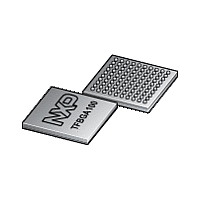
LPC1765FET100 NXP Semiconductors, LPC1765FET100 Datasheet - Page 11

LPC1765FET100
Manufacturer Part Number
LPC1765FET100
Description
The LPC1765 is a Cortex-M3 microcontroller for embedded applications featuring a high level of integration and low power consumption at frequencies of 100 MHz
Manufacturer
NXP Semiconductors
Datasheet
1.LPC1763FBD100.pdf
(82 pages)
Available stocks
Company
Part Number
Manufacturer
Quantity
Price
Company:
Part Number:
LPC1765FET100
Manufacturer:
EVERSPIN
Quantity:
5 000
Part Number:
LPC1765FET100
Manufacturer:
NXP/恩智浦
Quantity:
20 000
Company:
Part Number:
LPC1765FET100,551
Manufacturer:
Maxim
Quantity:
37
Company:
Part Number:
LPC1765FET100,551
Manufacturer:
NXP Semiconductors
Quantity:
10 000
NXP Semiconductors
Table 4.
LPC1769_68_67_66_65_64_63
Product data sheet
Symbol
P0[24]/AD0[1]/
I2SRX_WS/
CAP3[1]
P0[25]/AD0[2]/
I2SRX_SDA/
TXD3
P0[26]/AD0[3]/
AOUT/RXD3
P0[27]/SDA0/
USB_SDA
P0[28]/SCL0/
USB_SCL
P0[29]/USB_D+
P0[30]/USB_D
P1[0] to P1[31]
P1[0]/
ENET_TXD0
P1[1]/
ENET_TXD1
P1[4]/
ENET_TX_EN
P1[8]/
ENET_CRS
Pin description
Pin
8
7
6
25
24
30
95
94
93
92
29
[2]
[2]
[3]
[4]
[4]
[5]
[5]
[1]
[1]
[1]
[1]
…continued
Ball
D1
D2
D3
J2
J1
J3
G4
D5
B4
A4
C5
[4]
[4]
[5]
[1]
[1]
[2]
[2]
[3]
[1]
[1]
[5]
All information provided in this document is subject to legal disclaimers.
Type
I/O
I
I/O
I
I/O
I
I/O
O
I/O
I
O
I
I/O
I/O
I/O
I/O
I/O
I/O
I/O
I/O
I/O
I/O
I/O
I/O
O
I/O
O
I/O
O
I/O
I
Rev. 8 — 14 November 2011
Description
P0[24] — General purpose digital input/output pin.
AD0[1] — A/D converter 0, input 1.
I2SRX_WS — Receive Word Select. It is driven by the master and
received by the slave. Corresponds to the signal WS in the I
specification. (LPC1769/68/67/66/65/63 only).
CAP3[1] — Capture input for Timer 3, channel 1.
P0[25] — General purpose digital input/output pin.
AD0[2] — A/D converter 0, input 2.
I2SRX_SDA — Receive data. It is driven by the transmitter and read
by the receiver. Corresponds to the signal SD in the I
specification. (LPC1769/68/67/66/65/63 only).
TXD3 — Transmitter output for UART3.
P0[26] — General purpose digital input/output pin.
AD0[3] — A/D converter 0, input 3.
AOUT — DAC output (LPC1769/68/67/66/65/63 only).
RXD3 — Receiver input for UART3.
P0[27] — General purpose digital input/output pin. Output is
open-drain.
SDA0 — I
compliance).
USB_SDA — USB port I
LPC1769/68/66/65 only).
P0[28] — General purpose digital input/output pin. Output is
open-drain.
SCL0 — I
compliance).
USB_SCL — USB port I
LPC1769/68/66/65 only).
P0[29] — General purpose digital input/output pin.
USB_D+ — USB bidirectional D+ line. (LPC1769/68/66/65/64 only).
P0[30] — General purpose digital input/output pin.
USB_D — USB bidirectional D line. (LPC1769/68/66/65/64 only).
Port 1: Port 1 is a 32-bit I/O port with individual direction controls for
each bit. The operation of port 1 pins depends upon the pin function
selected via the pin connect block. Pins 2, 3, 5, 6, 7, 11, 12, and 13 of
this port are not available.
P1[0] — General purpose digital input/output pin.
ENET_TXD0 — Ethernet transmit data 0. (LPC1769/68/67/66/64 only).
P1[1] — General purpose digital input/output pin.
ENET_TXD1 — Ethernet transmit data 1. (LPC1769/68/67/66/64 only).
P1[4] — General purpose digital input/output pin.
ENET_TX_EN — Ethernet transmit data enable.
(LPC1769/68/67/66/64 only).
P1[8] — General purpose digital input/output pin.
ENET_CRS — Ethernet carrier sense. (LPC1769/68/67/66/64 only).
LPC1769/68/67/66/65/64/63
2
2
C0 clock input/output. Open-drain output (for I
C0 data input/output. Open-drain output (for I
2
2
C serial clock (OTG transceiver,
C serial data (OTG transceiver,
32-bit ARM Cortex-M3 microcontroller
© NXP B.V. 2011. All rights reserved.
2
S-bus
2
2
C-bus
C-bus
2
S-bus
11 of 82


