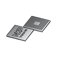
LPC3130_3131 NXP Semiconductors, LPC3130_3131 Datasheet - Page 15

LPC3130_3131
Manufacturer Part Number
LPC3130_3131
Description
The NXP LPC3130/3131 combine an 180 MHz ARM926EJ-S CPU core, high-speed USB2
Manufacturer
NXP Semiconductors
Datasheet
1.LPC3130_3131.pdf
(68 pages)
- Current page: 15 of 68
- Download datasheet (301Kb)
NXP Semiconductors
LPC3130_3131_1
Preliminary data sheet
6.3 JTAG
6.4 NAND flash controller
The Joint Test Action Group (JTAG) interface allows the incorporation of the
LPC3130/3131 in a JTAG scan chain.
This module has the following features:
The NAND flash controller is used as a dedicated interface to NAND flash devices.
Figure 4
module is formed by a controller block that controls the flow of data from/to the AHB bus
through the NAND flash controller block to/from the (external) NAND flash. An error
correction encoder/decoder (ECC enc/dec) module allows for hardware error correction
for support of Multi-Level Cell (MLC) NAND flash devices.
Before data is written from the buffer to the NAND flash, optionally it is first protected by
an error correction code generated by the ECC module. After data is read from the NAND
flash, the error correction module corrects any errors.
This module has the following features:
Fig 4. Block diagram of the NAND flash controller
•
•
•
•
•
ARM926 debug access
Boundary scan
Dedicated NAND flash interface with hardware controlled read and write accesses.
Wear leveling support with 516 byte mode.
Software controlled command and address transfers to support wide range of flash
devices.
shows a block diagram of the NAND flash controller module. The heart of the
Rev. 1 — 9 February 2009
AHB MULTILAYER MATRIX
NAND INTERFACE
CONTROLLER
Low-cost, low-power ARM926EJ-S microcontrollers
BUFFER
ENCODER/
DECODER
ECC
DMA transfer request
LPC3130/3131
002aae127
© NXP B.V. 2009. All rights reserved.
15 of 68
Related parts for LPC3130_3131
Image
Part Number
Description
Manufacturer
Datasheet
Request
R

Part Number:
Description:
Manufacturer:
Philips Semiconductors (Acquired by NXP)
Datasheet:
Part Number:
Description:
NXP Semiconductors designed the LPC2420/2460 microcontroller around a 16-bit/32-bitARM7TDMI-S CPU core with real-time debug interfaces that include both JTAG andembedded trace
Manufacturer:
NXP Semiconductors
Datasheet:

Part Number:
Description:
NXP Semiconductors designed the LPC2458 microcontroller around a 16-bit/32-bitARM7TDMI-S CPU core with real-time debug interfaces that include both JTAG andembedded trace
Manufacturer:
NXP Semiconductors
Datasheet:
Part Number:
Description:
NXP Semiconductors designed the LPC2468 microcontroller around a 16-bit/32-bitARM7TDMI-S CPU core with real-time debug interfaces that include both JTAG andembedded trace
Manufacturer:
NXP Semiconductors
Datasheet:
Part Number:
Description:
NXP Semiconductors designed the LPC2470 microcontroller, powered by theARM7TDMI-S core, to be a highly integrated microcontroller for a wide range ofapplications that require advanced communications and high quality graphic displays
Manufacturer:
NXP Semiconductors
Datasheet:
Part Number:
Description:
NXP Semiconductors designed the LPC2478 microcontroller, powered by theARM7TDMI-S core, to be a highly integrated microcontroller for a wide range ofapplications that require advanced communications and high quality graphic displays
Manufacturer:
NXP Semiconductors
Datasheet:
Part Number:
Description:
The Philips Semiconductors XA (eXtended Architecture) family of 16-bit single-chip microcontrollers is powerful enough to easily handle the requirements of high performance embedded applications, yet inexpensive enough to compete in the market for hi
Manufacturer:
NXP Semiconductors
Datasheet:
Part Number:
Description:
The XA-S3 device is a member of Philips Semiconductors? XA(eXtended Architecture) family of high performance 16-bitsingle-chip microcontrollers
Manufacturer:
NXP Semiconductors
Datasheet:

Part Number:
Description:
The NXP BlueStreak LH75401/LH75411 family consists of two low-cost 16/32-bit System-on-Chip (SoC) devices
Manufacturer:
NXP Semiconductors
Datasheet:

Part Number:
Description:
The NXP LPC3141 combine a 270 MHz ARM926EJ-S CPU core, High-speed USB 2
Manufacturer:
NXP Semiconductors

Part Number:
Description:
The NXP LPC3143 combine a 270 MHz ARM926EJ-S CPU core, High-speed USB 2
Manufacturer:
NXP Semiconductors

Part Number:
Description:
The NXP LPC3152 combines an 180 MHz ARM926EJ-S CPU core, High-speed USB 2
Manufacturer:
NXP Semiconductors

Part Number:
Description:
The NXP LPC3154 combines an 180 MHz ARM926EJ-S CPU core, High-speed USB 2
Manufacturer:
NXP Semiconductors

Part Number:
Description:
Standard level N-channel enhancement mode Field-Effect Transistor (FET) in a plastic package using NXP High-Performance Automotive (HPA) TrenchMOS technology
Manufacturer:
NXP Semiconductors
Datasheet:


