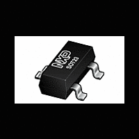
BSH201 NXP Semiconductors, BSH201 Datasheet

BSH201
Available stocks
Related parts for BSH201
BSH201 Summary of contents
Page 1
... This device has low threshold voltage and extremely fast switching making it ideal for battery powered applications and high speed digital interfacing. The BSH201 is supplied in the SOT23 subminiature surface mounting package. LIMITING VALUES Limiting values in accordance with the Absolute Maximum System (IEC 134) ...
Page 2
... Resistive load - MHz GS DS CONDITIONS ˚ -0. -0.25 A; -dI /dt = 100 - Product specification BSH201 MIN. TYP. MAX. UNIT - -1 150˚C -0 2.1 2.5 - 2.7 3.75 - 3.6 4.25 0.1 0. 100 - -50 -100 = 150˚ ...
Page 3
... j-a p Drain current, ID (A) BSH201 VGS = -10 V -2.5 V -2 -0.5 -1 -1.5 Drain-Source Voltage, VDS ( f(V ); parameter -1.5 V -1.7 V -1.9 V -2.1 V -2.3 V -2.5 V VGS = -10 V -0.1 -0.2 -0.3 -0.4 Drain Current, ID (A) PHP222 R = f(I ); parameter V DS(ON BSH201 D = tp/T T 1E+00 1E+01 /T -4.5 V -2.3 V -1 ˚ -4 ˚ Rev 1.000 ...
Page 4
... -2.5 -2 -1.5 Gate-Source Voltage, VGS (V) Fig.11. Sub-threshold drain current f(V ; conditions ˚C D GS) j Capacitances, Ciss, Coss, Crss (pF) -0.1 -1.0 -10.0 Drain-Source Voltage, VDS ( iss ); conditions MHz DS GS BSH201 125 150 = BSH201 Ciss Coss Crss -100 oss rss Rev 1.000 ...
Page 5
... Gate charge, (nC) Fig.13. Typical turn-on gate-charge characteristics f August 1998 BSH201 Source-Drain Diode Current, IF (A) 3.5 3 2.5 2 1 Fig.14. Typical reverse diode current f(V F SDS 5 Product specification BSH201 BSH201 150 0.5 1 1.5 Drain-Source Voltage, VSDS (V) ); conditions parameter T GS Rev 1.000 2 j ...
Page 6
... scale 0.48 0.15 3.0 1.4 2.5 0.45 1.9 0.95 0.38 0.09 2.8 1.2 2.1 0.15 REFERENCES IEC JEDEC EIAJ Fig.15. SOT23 surface mounting package. 6 Product specification SOT23 detail 0.55 0.2 0.1 0.45 EUROPEAN ISSUE DATE PROJECTION 97-02-28 BSH201 Rev 1.000 ...
Page 7
... Philips customers using or selling these products for use in such applications their own risk and agree to fully indemnify Philips for any damages resulting from such improper use or sale. August 1998 7 Product specification BSH201 Rev 1.000 ...


