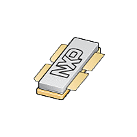
BLF2425M6LS180P NXP Semiconductors, BLF2425M6LS180P Datasheet

BLF2425M6LS180P
Available stocks
Related parts for BLF2425M6LS180P
BLF2425M6LS180P Summary of contents
Page 1
... BLF2425M6L180P; BLF2425M6LS180P Power LDMOS transistor Rev. 1 — 7 February 2012 1. Product profile 1.1 General description 180 W LDMOS power transistor for various applications such as ISM and industrial heating at frequencies from 2400 MHz to 2500 MHz. Table 1. RF performance at T Test signal CW 1.2 Features and benefits ...
Page 2
... BLF2425M6L180P (SOT539A BLF2425M6LS180P (SOT539B [1] Connected to flange. 3. Ordering information Table 3. Type number BLF2425M6L180P BLF2425M6LS180P - 4. Limiting values Table 4. In accordance with the Absolute Maximum Rating System (IEC 60134). Symbol stg T case T j BLF2425M6L180P_25M6LS180P Objective data sheet Pinning ...
Page 3
... Test information 7.1 Ruggedness in class-AB operation The BLF2425M6L180P and BLF2425M6LS180P are capable of withstanding a load mismatch corresponding to VSWR = <tbd> through all phases under the following conditions: V BLF2425M6L180P_25M6LS180P Objective data sheet Thermal characteristics Parameter thermal resistance from junction to case DC characteristics C per section ...
Page 4
... NXP Semiconductors 7.2 Impedance information Table 8. Measured load-pull data. Typical values per section. Z and (MHz) 2400 2450 2500 Fig 1. BLF2425M6L180P_25M6LS180P Objective data sheet Typical impedance defined in Figure () 5.9 j8.0 8.4 j7.6 10.6 j5.8 gate Definition of transistor impedance All information provided in this document is subject to legal disclaimers. ...
Page 5
... NXP Semiconductors 7.3 Test circuit Fig 2. Table 9. For test circuit, see Component C1, C2, C3 C4, C5, C10, C11 C6, C12, C13 C7 C8, C9 C14 R1, R2 [1] American technical ceramics type 100A or capacitor of same quality. [2] American technical ceramics type 800B or capacitor of same quality. [3] American technical ceramics type 100B or capacitor of same quality. ...
Page 6
... NXP Semiconductors 8. Package outline Flanged balanced LDMOST ceramic package; 2 mounting holes; 4 leads DIMENSIONS (millimetre dimensions are derived from the original inch dimensions) c UNIT 11.81 4.7 0.18 31.55 31.52 mm 4.2 11.56 0.10 30.94 30.96 0.185 0.465 1.242 1.241 0.007 inches 0.165 0.455 1.218 1.219 0.004 Note 1. millimeter dimensions are derived from the original inch dimensions. ...
Page 7
... NXP Semiconductors Earless flanged balanced LDMOST ceramic package; 4 leads Dimensions (1) Unit max 4.7 11.81 0.18 31.55 mm nom min 4.2 11.56 0.10 30.94 max 0.185 0.465 0.007 1.242 mm nom min 0.165 0.455 0.004 1.218 Note 1. millimeter dimensions are derived from the original inch dimensions. Outline version ...
Page 8
... NXP Semiconductors 9. Handling information CAUTION This device is sensitive to ElectroStatic Discharge (ESD). Observe precautions for handling electrostatic sensitive devices. Such precautions are described in the ANSI/ESD S20.20, IEC/ST 61340-5, JESD625-A or equivalent standards. 10. Abbreviations Table 10. Acronym CW DC ESD ISM LDMOS LDMOST RF SMD VSWR 11. Revision history Table 11 ...
Page 9
... Terms and conditions of commercial sale of NXP Semiconductors. Right to make changes — NXP Semiconductors reserves the right to make changes to information published in this document, including without limitation specifications and product descriptions, at any time and without notice ...
Page 10
... NXP Semiconductors’ specifications such use shall be solely at customer’s own risk, and (c) customer fully indemnifies NXP Semiconductors for any liability, damages or failed product claims resulting from customer design and use of the product for automotive applications beyond NXP Semiconductors’ ...
Page 11
... NXP Semiconductors 14. Contents 1 Product profile . . . . . . . . . . . . . . . . . . . . . . . . . . 1 1.1 General description . . . . . . . . . . . . . . . . . . . . . 1 1.2 Features and benefits . . . . . . . . . . . . . . . . . . . . 1 1.3 Applications . . . . . . . . . . . . . . . . . . . . . . . . . . . 1 2 Pinning information . . . . . . . . . . . . . . . . . . . . . . 2 3 Ordering information . . . . . . . . . . . . . . . . . . . . . 2 4 Limiting values Thermal characteristics . . . . . . . . . . . . . . . . . . 3 6 Characteristics . . . . . . . . . . . . . . . . . . . . . . . . . . 3 7 Test information . . . . . . . . . . . . . . . . . . . . . . . . . 3 7.1 Ruggedness in class-AB operation . . . . . . . . . 3 7.2 Impedance information . . . . . . . . . . . . . . . . . . . 4 7.3 Test circuit Package outline . . . . . . . . . . . . . . . . . . . . . . . . . 6 9 Handling information Abbreviations ...


