BLF6G27LS-50BN NXP Semiconductors, BLF6G27LS-50BN Datasheet
BLF6G27LS-50BN


Related parts for BLF6G27LS-50BN


BLF6G27LS-50BN Summary of contents
Page 1
... BLF6G27L-50BN; BLF6G27LS-50BN Power LDMOS transistor Rev. 2 — 7 April 2011 1. Product profile 1.1 General description 50 W LDMOS power transistor for base station applications at frequencies from 2500 MHz to 2700 MHz. Table 1. RF performance at T Mode of operation 2-carrier W-CDMA [1] Test signal: 3GPP; test model 1; 64 DPCH; PAR = 8 0.01 % probability on CCDF per carrier; ...
Page 2
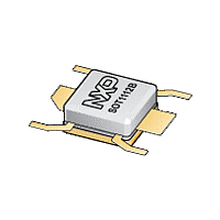
... NXP Semiconductors 2. Pinning information Table 2. Pin BLF6G27L-50BN (SOT1112A BLF6G27LS-50BN (SOT1112B [1] Connected to flange. 3. Ordering information Table 3. Type number BLF6G27L-50BN BLF6G27LS-50BN 4. Limiting values Table 4. In accordance with the Absolute Maximum Rating System (IEC 60134). Symbol V DS ...
Page 3
... NXP Semiconductors 5. Thermal characteristics Table 5. Symbol Parameter R th(j-case) 6. Characteristics Table 6. ° Symbol Parameter V (BR)DSS V GS(th DSS I DSX I GSS DS(on) 7. Application information Table 7. All testing performed in Class-AB production test circuit; test signal 3GPP; test model 1; 64 DPCH; PAR = 8 0.01 % probability on CCDF per carrier; carrier spacing 5 MHz 2600 MHz ...
Page 4
... DS Symbol PAR O 7.1 Ruggedness in Class-AB operation The BLF6G27L-50BN and BLF6G27LS-50BN are capable of withstanding a load mismatch corresponding to VSWR = through all phases under the following conditions: V 7.2 Single carrier IS-95 Single carrier IS-95 with pilot, paging, sync and 6 traffic channels (Walsh codes 8 - 13). PAR = 9 0.01 % probability on the CCDF. Channel bandwidth is 1.2288 MHz. ...
Page 5
... NXP Semiconductors 20 ACPR 885 (dBc) (1) 30 (2) ( 430 mA ( 2500 MHz ( 2600 MHz ( 2700 MHz Fig 3. Single carrier IS-95 ACPR at 885 kHz as a function of load power; typical values 10 PAR 430 mA ...
Page 6
... NXP Semiconductors (dB (1) (2) ( 430 mA ( 2500 MHz ( 2600 MHz ( 2700 MHz Fig 7. Pulsed CW power gain as a function of load power; typical values BLF6G27L-50BN_6G27LS-50BN Product data sheet 001aan487 (W) L Fig 8. ...
Page 7
... NXP Semiconductors 7.4 2-carrier W-CDMA All testing performed in Class-AB production test circuit; test signal 3GPP; test model 1; 64 DPCH; PAR = 8 0.01 % probability on CCDF per carrier; carrier spacing 5 MHz 2500 MHz 17 (dB) 16.5 16.0 (1) 15.5 (2) (3) 15.0 14 430 mA ( 2500 MHz ...
Page 8
... NXP Semiconductors 0 ACPR 5M (dBc) 10 (1) ( 430 mA ( 2500 MHz ( 2600 MHz ( 2700 MHz Fig 11. 2-carrier W-CDMA ACPR at 5 MHz as a function of load power; typical values BLF6G27L-50BN_6G27LS-50BN Product data sheet 001aan491 ACPR (dBc) ...
Page 9
... NXP Semiconductors 7.5 Single carrier W-CDMA All testing performed in Class-AB production test circuit; test signal 3GPP; test model 1; 64 DPCH; PAR = 7 0.01 % probability on CCDF per carrier 2700 MHz °C; unless otherwise specified. T case 9.0 PAR 7.5 6.0 (1) (2) 4.5 (3) 3.0 1 430 mA ( 2500 MHz ...
Page 10
... NXP Semiconductors 8. Package outline Flanged ceramic package; 2 mounting holes; 6 leads Dimensions (1) Unit max 4.65 1.14 5.26 0.18 mm nom min 3.76 0.89 5.00 0.10 max 0.183 0.045 0.207 0.007 inches nom min 0.148 0.035 0.197 0.004 Note 1. millimeter dimensions are derived from the original inch dimensions. ...
Page 11
... NXP Semiconductors Earless flanged ceramic package; 6 leads Dimensions (1) Unit max 4.65 1.14 5.26 0.18 mm nom min 3.76 0.89 5.00 0.10 max 0.183 0.045 0.207 0.007 inches nom min 0.148 0.035 0.197 0.004 Note 1. millimeter dimensions are derived from the original inch dimensions. 2. dimension is measured 0.030 inch (0.76 mm) from the body. ...
Page 12
... NXP Semiconductors 9. Handling information CAUTION This device is sensitive to ElectroStatic Discharge (ESD). Observe precautions for handling electrostatic sensitive devices. Such precautions are described in the ANSI/ESD S20.20, IEC/ST 61340-5, JESD625-A or equivalent standards. 10. Abbreviations Table 9. Acronym 3GPP CCDF CW DPCH ESD LDMOS PAR RF VSWR W-CDMA ...
Page 13
... NXP Semiconductors 11. Revision history Table 10. Revision history Document ID BLF6G27L-50BN_6G27LS-50BN v.2 Modifications: BLF6G27L-50BN_6G27LS-50BN v.1 BLF6G27L-50BN_6G27LS-50BN Product data sheet Release date Data sheet status 20110407 Product data sheet • Section 1.1 on page has been changed • Table 1 on page 1: several changes have been made. ...
Page 14
... NXP Semiconductors and its customer, unless NXP Semiconductors and customer have explicitly agreed otherwise in writing event however, shall an agreement be valid in which the NXP Semiconductors product is deemed to offer functions and qualities beyond those described in the Product data sheet. ...
Page 15
... Product data sheet NXP Semiconductors’ specifications such use shall be solely at customer’s own risk, and (c) customer fully indemnifies NXP Semiconductors for any liability, damages or failed product claims resulting from customer design and use of the product for automotive applications beyond NXP Semiconductors’ ...
Page 16
... NXP Semiconductors 14. Contents 1 Product profile . . . . . . . . . . . . . . . . . . . . . . . . . . 1 1.1 General description . . . . . . . . . . . . . . . . . . . . . 1 1.2 Features and benefits . . . . . . . . . . . . . . . . . . . . 1 1.3 Applications . . . . . . . . . . . . . . . . . . . . . . . . . . . 1 2 Pinning information . . . . . . . . . . . . . . . . . . . . . . 2 3 Ordering information . . . . . . . . . . . . . . . . . . . . . 2 4 Limiting values Thermal characteristics . . . . . . . . . . . . . . . . . . 3 6 Characteristics . . . . . . . . . . . . . . . . . . . . . . . . . . 3 7 Application information 7.1 Ruggedness in Class-AB operation . . . . . . . . . 4 7.2 Single carrier IS- 7.3 Pulsed 7.4 2-carrier W-CDMA . . . . . . . . . . . . . . . . . . . . . . 7 7.5 Single carrier W-CDMA . . . . . . . . . . . . . . . . . . 9 8 Package outline . . . . . . . . . . . . . . . . . . . . . . . . 10 9 Handling information ...