LM339AMX/NOPB National Semiconductor, LM339AMX/NOPB Datasheet - Page 4
LM339AMX/NOPB
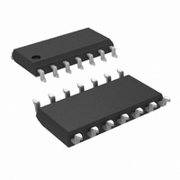
Manufacturer Part Number
LM339AMX/NOPB
Description
IC COMPARATOR QUAD LO PWR 14SOIC
Manufacturer
National Semiconductor
Type
General Purposer
Specifications of LM339AMX/NOPB
Number Of Elements
4
Output Type
CMOS, DTL, ECL, MOS, Open-Collector, TTL
Voltage - Supply
2 V ~ 36 V, ±1 V ~ 18 V
Mounting Type
Surface Mount
Package / Case
14-SOIC (0.154", 3.90mm Width)
Comparator Type
Precision
No. Of Comparators
4
Response Time
1.3µs
Ic Output Type
CMOS, MOS, TTL, DTL, ECL
Supply Current
800µA
Supply Voltage Range
± 1V To ± 18V
Rohs Compliant
Yes
Number Of Elements
4
Technology
Bipolar
Input Offset Voltage
2mV
Input Bias Current (typ)
250nA
Single Supply Voltage (typ)
3/5/9/12/15/18/24/28V
Dual Supply Voltage (typ)
±3/±5/±9/±12/±15V
Supply Current (max)
2@5VmA
Power Supply Requirement
Single/Dual
Voltage Gain In Db
106.02dB
Single Supply Voltage (min)
2V
Single Supply Voltage (max)
36V
Dual Supply Voltage (min)
±1V
Dual Supply Voltage (max)
±18V
Power Dissipation
760mW
Operating Temp Range
0C to 70C
Operating Temperature Classification
Commercial
Mounting
Surface Mount
Pin Count
14
Package Type
SOIC N
Lead Free Status / RoHS Status
Lead free / RoHS Compliant
Other names
LM339AMX
LM339AMXTR
LM339AMXTR
Available stocks
Company
Part Number
Manufacturer
Quantity
Price
Company:

Part Number:
LM339AMX/NOPB
Manufacturer:
TI
Quantity:
12 400
Part Number:
LM339AMX/NOPB
Manufacturer:
NS/国半
Quantity:
20 000


www.national.com
Saturation Voltage
Output Leakage Current
Differential Input Voltage
Input Offset Voltage
Input Offset Current
Input Bias Current
Input Common-Mode
Voltage Range
Saturation Voltage
Output Leakage Current V
Differential Input Voltage Keep all V
Electrical Characteristics
(V
Electrical Characteristics
(V
Note 1: For operating at high temperatures, the LM339/LM339A, LM2901, LM3302 must be derated based on a 125˚C maximum junction temperature and a
thermal resistance of 95˚C/W which applies for the device soldered in a printed circuit board, operating in a still air ambient. The LM239 and LM139 must be derated
based on a 150˚C maximum junction temperature. The low bias dissipation and the “ON-OFF” characteristic of the outputs keeps the chip dissipation very small
(P
Note 2: Short circuits from the output to V
current is approximately 20 mA independent of the magnitude of V
Note 3: This input current will only exist when the voltage at any of the input leads is driven negative. It is due to the collector-base junction of the input PNP
transistors becoming forward biased and thereby acting as input diode clamps. In addition to this diode action, there is also lateral NPN parasitic transistor action
on the IC chip. This transistor action can cause the output voltages of the comparators to go to the V
duration that an input is driven negative. This is not destructive and normal output states will re-establish when the input voltage, which was negative, again returns
to a value greater than −0.3 V
Note 4: These specifications are limited to −55˚C ≤ T
−25˚C ≤ T
≤ +85˚C.
Note 5: The direction of the input current is out of the IC due to the PNP input stage. This current is essentially constant, independent of the state of the output so
no loading change exists on the reference or input lines.
Note 6: The input common-mode voltage or either input signal voltage should not be allowed to go negative by more than 0.3V. The upper end of the common-mode
voltage range is V
Note 7: The response time specified is a 100 mV input step with 5 mV overdrive. For larger overdrive signals 300 ns can be obtained, see typical performance
characteristics section.
Note 8: Positive excursions of input voltage may exceed the power supply level. As long as the other voltage remains within the common-mode range, the
comparator will provide a proper output state. The low input voltage state must not be less than −0.3 V
supply, if used) (at 25˚C).
Note 9: At output switch point, V
For LM3302, V
Note 10: Refer to RETS139AX for LM139A military specifications and to RETS139X for LM139 military specifications.
D
+
+
≤100 mW), provided the output transistors are allowed to saturate.
= 5.0 V
= 5.0 V
Parameter
Parameter
A
≤ +85˚C, the LM339/LM339A temperature specifications are limited to 0˚C ≤ T
DC
DC
+
from 5 V
, (Note 4))
, (Note 4))
+
−1.5V at 25˚C, but either or both inputs can go to +30 V
DC
to 28 V
DC
(Note 9)
I
I
Linear Range, V
V
(Note 6)
V
I
V
if used), (Note 8)
IN(+)
IN(+)
SINK
+
IN(−)
IN(+) =
O
O
(at 25˚)C.
.1.4 V
= 30 V
= 30 V
V
I
V
V
V
Keep all V
if used), (Note 8)
DC
−I
SINK
or I
≤ 4 mA
IN(−)
IN(+) =
O
O
= 1 V
IN(−)
.
= 30 V
= 28 V
1 V
DC
IN(−)
+
=1 V
≤ 4 mA
DC
can cause excessive heating and eventual destruction. When considering short circuits to ground, the maximum output
, V
DC
IN
, R
DC
DC
1 V
’s ≥ 0 V
S
, (LM3302, V
CM
(LM3302, V
with Output in
Conditions
, V
= 0Ω with V
, V
DC
DC
DC
IN
DC
Conditions
’s ≥ 0 V
CM
IN(−)
= 0V
, V
IN(+)
, (LM3302,
)
, V
A
(Continued)
IN(+)
= 0V (Note 5)
DC
≤ +125˚C, for the LM139/LM139A. With the LM239/LM239A, all temperature specifications are limited to
IN(−)
= 0,
= 0,
(or V
+
DC
= 0,
from 5 V
+
= 0,
= 28 V
O
(or V
−
+
= 28 V
.
,
DC
−
,
DC
to 30 V
DC
DC
)
)
without damage (25V for LM3302), independent of the magnitude of V
4
DC
Min Typ
Min Typ
; and over the full input common-mode range (0 V
LM239, LM339
LM139A
A
≤ +70˚C, and the LM2901, LM3302 temperature range is −40˚C ≤ T
V
Max
700
1.0
Max
36
+
150
400
700
9.0
1.0
36
−2.0
+
voltage level (or to ground for a large overdrive) for the time
DC
LM239A, LM339A
Min Typ
(or 0.3 V
Min Typ
0
LM2901
200
400
50
DC
9
below the magnitude of the negative power
V
Max
200
500
+
700
Max
1.0
700
15
36
1.0
−2.0
36
Min Typ
Min Typ
DC
0
to V
LM3302
LM139
+
−1.5 V
V
1000
Max
Max
700
+
300
700
1.0
1.0
36
40
28
DC
−2.0
+
), at 25˚C.
.
mV
mV
mV
Units
Units
µA
nA
nA
µA
V
V
V
DC
DC
DC
A
DC
DC
DC
DC
DC
DC
DC
Related parts for LM339AMX/NOPB
Image
Part Number
Description
Manufacturer
Datasheet
Request
R

Part Number:
Description:
IC,VOLT COMPARATOR,QUAD,BIPOLAR,SOP,14PIN,PLASTIC
Manufacturer:
National Semiconductor
Datasheet:


Part Number:
Description:
IC COMPARATOR QUAD LO PWR 14SOIC
Manufacturer:
National Semiconductor
Datasheet:


Part Number:
Description:
QUAD DIFFERENTIAL COMPARATOR
Manufacturer:
Unisonic Technologies Co., Ltd.
Part Number:
Description:
QUAD DIFFERENTIAL COMPARATOR
Manufacturer:
Unisonic Technologies Co., Ltd.
Part Number:
Description:
QUAD DIFFERENTIAL COMPARATOR
Manufacturer:
Unisonic Technologies Co., Ltd.
Part Number:
Description:
Low Power Low Offset Voltage Quad Comparators
Manufacturer:
National Semiconductor Corporation
Datasheet:
Part Number:
Description:
Quad Single Supply Comparator
Manufacturer:
Unisonic Technologies
Datasheet:

Part Number:
Description:
National Semiconductor [8-Bit D/A Converter]
Manufacturer:
National Semiconductor
Datasheet:
Part Number:
Description:
National Semiconductor [Media Coprocessor]
Manufacturer:
National Semiconductor
Datasheet:
Part Number:
Description:
Digitally Controlled Tone and Volume Circuit with Stereo Audio Power Amplifier, Microphone Preamp Stage and National 3D Sound
Manufacturer:
National Semiconductor
Datasheet:
Part Number:
Description:
Digitally Controlled Tone and Volume Circuit with Stereo Audio Power Amplifier, Microphone Preamp Stage and National 3D Sound
Manufacturer:
National Semiconductor
Datasheet:
Part Number:
Description:
AC97 Rev 2 Codec with Sample Rate Conversion and National 3D Sound
Manufacturer:
National Semiconductor