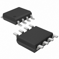
MAX971CSA+ Maxim Integrated Products, MAX971CSA+ Datasheet

MAX971CSA+
Specifications of MAX971CSA+
Related parts for MAX971CSA+
MAX971CSA+ Summary of contents
Page 1
... DIP/SO/µMAX No 16-Pin DIP/SO 8-Pin Yes DIP/SO/µMAX 8-Pin Yes DIP/SO/µMAX 8-Pin Yes DIP/SO/µMAX No 16-Pin DIP/SO UCSP is a trademark of Maxim Integrated Products, Inc. Features Applications Window Comparators Level Translators Oscillator Circuits Ordering Information TEMP RANGE PIN-PACKAGE + Plastic Dip + + µMAX ...
Page 2
Ultra-Low-Power, Open-Drain, Single/Dual-Supply Comparators ABSOLUTE MAXIMUM RATINGS GND, GND to V-................................-0.3V, +12V Inputs Current: IN_+, IN_-, HYST..............................................20mA Voltage: IN_+, IN_-, HYST ...............(V+ + 0.3V) to (V- - 0.3V) Outputs Current: REF...................................................................20mA OUT_ ................................................................50mA Voltage: REF ...
Page 3
ELECTRICAL CHARACTERISTICS—5V OPERATION (continued) ( GND = 0V MIN A PARAMETER MAX9_2/MAX9_3, I Output Low Voltage MAX9_1/MAX9_4, I Output Leakage Current V REFERENCE (MAX9_1/MAX982/MAX9_3/MAX9_4 ONLY) MAX971/MAX973/ MAX974 Reference Voltage MAX981–MAX984 T ...
Page 4
Ultra-Low-Power, Open-Drain, Single/Dual-Supply Comparators ELECTRICAL CHARACTERISTICS—3V OPERATION (continued) ( GND = 0V MIN PARAMETER Response Time (High-to-Low T A Transition) 1M pullup to V+ Response Time (Low-to-High T A Transition) ...
Page 5
Operating Characteristics ( GND = 0V +25°C, unless otherwise noted.) A OUTPUT VOLTAGE LOW vs. LOAD CURRENT 2 2 1.5 1.0 0 ...
Page 6
Ultra-Low-Power, Open-Drain, Single/Dual-Supply Comparators ( GND = 0V +25°C, unless otherwise noted.) A MAX9_1/MAX972/MAX9_4 TRANSFER FUNCTION 5.0 +5V 4.5 10k 100k 3.5 3.0 2.5 2.0 1.5 1.0 0.5 0 ...
Page 7
PIN MAX971/ MAX972 MAX982 MAX981 DIP/SO/ DIP/SO/ DIP/SO/ UCSP µMAX µMAX µMAX 1 — — — — — — 4 — — — 5 — — — — ...
Page 8
Ultra-Low-Power, Open-Drain, Single/Dual-Supply Comparators PIN NAME MAX974 MAX984 1 OUTB 2 OUTA INA- 5 INA+ 6 INB- 7 INB+ 8 REF INC- 11 INC+ 12 IND- 13 IND+ 14 GND 15 OUTD 16 OUTC ...
Page 9
Detailed Description The MAX971–MAX974/MAX981–MAX984 comprise various combinations of a micropower 1.182V reference and micropower comparators. The Typical Operating Circuit shows the MAX971/MAX981 configuration, and Figures 1a–1d show the MAX9_2–MAX9_4 configurations. Internal hysteresis in the MAX9_1, MAX982, and MAX9_3 provides the ...
Page 10
Ultra-Low-Power, Open-Drain, Single/Dual-Supply Comparators THRESHOLDS IN+ HYSTERESIS IN- BAND REF HYST HB OUT Figure 2. Threshold Hysteresis Band Low-Voltage Operation The guaranteed minimum operating voltage is 2.5V (or ±1.25V). As the total supply ...
Page 11
Information Hysteresis increases the comparators’ noise margin by increasing the upper threshold and decreasing the lower threshold (Figure 2). Hysteresis (MAX9_1/MAX982/MAX9_3) To add hysteresis to the MAX9_1, MAX982, or MAX9_3, connect resistor R1 between REF and HYST, and connect ...
Page 12
Ultra-Low-Power, Open-Drain, Single/Dual-Supply Comparators 2) Select R1. The leakage current into INB- is normally under 1nA, so the current through R1 should exceed 100nA for the thresholds to be accurate. R1 values up to about 10M can be used, but ...
Page 13
WALL ADAPTER 9V DC STEP-DOWN REGULATOR Q1 1M BATTERY (4 CELLS) MAX973 MAX983 953k 4 INB- 470k 1 OUTA 110k 3 INA+ R2 47k Figure 6. Battery Switchover Circuit UCSP Applications Information For the latest application details ...
Page 14
Ultra-Low-Power, Open-Drain, Single/Dual-Supply Comparators TOP VIEW GND 1 8 OUT MAX971 IN REF MAX981 IN HYST DIP/SO/ MAX TOP VIEW (BUMPS ON BOTTOM OUTA V+ OUTB B INA- ...
Page 15
PART TEMP RANGE MAX971EPA - +85 C MAX971ESA - +85 C MAX972CPA +70 C MAX972CSA +70 C MAX972CUA +70 C MAX972EBL-T* - +85 C MAX972EPA ...
Page 16
Ultra-Low-Power, Open-Drain, Single/Dual-Supply Comparators (The package drawing(s) in this data sheet may not reflect the most current specifications. For the latest package outline information www.maxim-ic.com/packages.) 16 ______________________________________________________________________________________ Package Information ...
Page 17
... Maxim cannot assume responsibility for use of any circuitry other than circuitry entirely embodied in a Maxim product. No circuit patent licenses are implied. Maxim reserves the right to change the circuitry and specifications without notice at any time. Maxim Integrated Products, 120 San Gabriel Drive, Sunnyvale, CA 94086 408-737-7600 ____________________ 17 © 2003 Maxim Integrated Products ...


