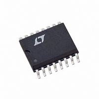
LT1017CSW Linear Technology, LT1017CSW Datasheet

LT1017CSW
Specifications of LT1017CSW
Available stocks
Related parts for LT1017CSW
LT1017CSW Summary of contents
Page 1
... Available in 8-Lead PDIP , 8-Lead Plastic S0, and 16-Lead Plastic SO Packages APPLICATIONS n Power Supply Monitors n Relay Driving n Oscillators L, LT, LTC and LTM are registered trademarks of Linear Technology Corporation. All other trademarks are the property of their respective owners. TYPICAL APPLICATION 1.5V Powered Refrigerator Alarm + V 1.5V 665k 1% ...
Page 2
... Lead Temperature (Soldering, 10 sec) ................. 300°C 8 – OUT OUT B ORDER PART NUMBER 1017 LT1017CN8 1017I LT1017IN8 1018 LT1018CN8 1018I OUTPUT B 6 – 45°C/W JC PART MARKING ORDER PART NUMBER LT1017CSW LT1018CSW TOP VIEW + OUTPUT – OUTPUT B 7 – + – – – +IN B ...
Page 3
ELECTRICAL CHARACTERISTICS temperature range of – 55°C to 85°C for M grade parts, –40°C to 85°C for I grade parts and 0°C to 70°C for C grade parts. PARAMETER CONDITIONS Offset Voltage ± 0.75V ≤ V (Note 2) Bias Current ...
Page 4
LT1017/LT1018 ELECTRICAL CHARACTERISTICS temperature range of – 55°C to 85°C for M grade parts, –40°C to 85°C for I grade parts and 0°C to 70°C for C grade parts. PARAMETER CONDITIONS Leakage Current ≥ ...
Page 5
TYPICAL PERFORMANCE CHARACTERISTICS Input Bias Current 100 – LT1018 LT1018 – – LT1017 BIAS REVERSES POLARITY + LT1017 – ...
Page 6
LT1017/LT1018 TYPICAL PERFORMANCE CHARACTERISTICS Output Sinking Current Limit 100 + OUTPUT SHORTED TO V LT1018 LT1017 LT1018 V = 40V S 40 LT1017 V = 40V –50 ...
Page 7
TYPICAL APPLICATIONS Driving Relays 12V – LT1017 1017/18 TA03 Increasing Positive Output Current + LT1017/ LT1018 2 – 1N4148 4 – ...
Page 8
LT1017/LT1018 TYPICAL APPLICATIONS LT1004 8 Negative Voltage Regulator 510k 2.5V 2 150pF 8 510k – 1 LT1017/ LT1018 3 220μ 100k 1k 220pF 1017/18 TA08 2-Wire Comparator 1N4148 × LT1018 2 ...
Page 9
TYPICAL APPLICATIONS LT1034 1.235V LT1009 2.5V 5V Power Supply Monitor 36. 2.5k 1/2 LT1017 1% 6 – 1/2 LT1017 2 – 4 OUTPUT VALID 11.2k FOR V 1% 1017/18 TA10 Precise ...
Page 10
LT1017/LT1018 TYPICAL APPLICATIONS 2M 1M 110k LT1004 1.2V 10 Power Supply Monitor V IN 160k 330Ω 1N4148 100k 2 8 – LT1018 1μ LT1004 390k 1.2V 1N4148 120k V IN 6.00V 5.25V FLASH AT 1Hz ...
Page 11
TYPICAL APPLICATIONS LT1004 5 + 1/2 LT1018 6 – FULL-SCALE TRIM 100k INPUT Regulated Step-Up Converter 5V 400mH** 1N4148 100k 2 8 – 1N4148 0.1μF 1 1/2 LT1018 200k 1.2V 2000pF 910k 7 ( ...
Page 12
LT1017/LT1018 PACKAGE DESCRIPTION SEATING SEATING PLANE PLANE 45° 45° Package H Package 8-Lead TO-5 Metal Can (.200 Inch PCD) 8-Lead TO-5 Metal Can (.200 Inch PCD) (Reference LTC DWG # 05-08-1320) (Reference LTC DWG # 05-08-1320) .335 – ...
Page 13
PACKAGE DESCRIPTION .300 – .325 (7.620 – 8.255) .008 – .015 (0.203 – 0.381) +.035 .325 –.015 ( ) +0.889 8.255 –0.381 NOTE: 1. DIMENSIONS ARE MILLIMETERS *THESE DIMENSIONS DO NOT INCLUDE MOLD FLASH OR PROTRUSIONS. MOLD FLASH OR PROTRUSIONS ...
Page 14
LT1017/LT1018 PACKAGE DESCRIPTION .050 BSC .245 MIN .030 ±.005 TYP RECOMMENDED SOLDER PAD LAYOUT .010 – .020 (0.254 – 0.508) .008 – .010 (0.203 – 0.254) (0.406 – 1.270) NOTE: 1. DIMENSIONS IN 2. DRAWING NOT TO SCALE 3. THESE ...
Page 15
... MOLD FLASH OR PROTRUSIONS SHALL NOT EXCEED .006" (0.15mm) Information furnished by Linear Technology Corporation is believed to be accurate and reliable. However, no responsibility is assumed for its use. Linear Technology Corporation makes no representa- tion that the interconnection of its circuits as described herein will not infringe on existing patent rights. ...
Page 16
... INTERROGATE PULSE OUTPUT PULSE V > TRIP NO OUTPUT PULSE FOR V < TRIP 20k OUTPUT 200pF , 25nA I , 3nA I , 250ns t OS(MAX) B(MAX) OS(MAX) PD(MAX) , 2.5V Reference Voltage , Rail-to-Rail Input OS(MAX) , 2.5V Reference Voltage , 80ns 0208 REV F • PRINTED IN USA © LINEAR TECHNOLOGY CORPORATION 2008 10178ff ...


