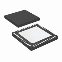
LMH0036SQX/NOPB National Semiconductor, LMH0036SQX/NOPB Datasheet - Page 6

LMH0036SQX/NOPB
Manufacturer Part Number
LMH0036SQX/NOPB
Description
IC RECLOCKER SD 4:1 MUX 48LLP
Manufacturer
National Semiconductor
Type
Reclockerr
Datasheet
1.LMH0036SQENOPB.pdf
(14 pages)
Specifications of LMH0036SQX/NOPB
Applications
SDTV/HDTV
Mounting Type
Surface Mount
Package / Case
48-LLP
Lead Free Status / RoHS Status
Lead free / RoHS Compliant
Other names
LMH0036SQX
www.national.com
Symbol
BW
TOL
TOL
AC Electrical Characteristics
Over Supply Voltage and Operating Temperature ranges, unless otherwise specified. (Note 3)
Note 1: “Absolute Maximum Ratings” are those parameter values beyond which the life and operation of the device cannot be guaranteed. The stating herein of
these maximums shall not be construed to imply that the device can or should be operated at or beyond these values. The table of “Electrical Characteristics”
specifies acceptable device operating conditions.
Note 2: Current flow into device pins is defined as positive. Current flow out of device pins is defined as negative. All voltages are referenced to V
zero volts).
Note 3: Typical values are stated for: V
Note 4: Specification is guaranteed by design.
Note 5: R
Note 6: Measured from first SDI transition until Lock Detect (LD) output goes high (true).
Note 7: Peak-to-peak amplitude with sinusoidal modulation per SMPTE RP 184-1996 paragraph 4.1. The test data signal shall be color bars.
Note 8: This parameter is guaranteed by characterization over voltage and temperature limits.
Note 9: Refer to “A1” in Figure 1 of SMPTE RP 184-1996.
Note 10: Refer to “A2” in Figure 1 of SMPTE RP 184-1996.
Note 11: Serial Data Output Jitter is total output jitter with 0.2UI
BR
T
F
F
F
t
t
t
t
t
t
ACQ
r
r
r
r
REF
TOL
JIT
JIT
CO
, t
, t
, t
, t
LOOP
SD
JIT
JIT
f
f
f
f
L
= 100Ω differential.
Serial Data Rate
Serial Input Jitter
Tolerance
Serial Input Jitter
Tolerance
Serial Data Output Jitter
Loop Bandwidth
Serial Clock Output
Frequency
Serial Clock Output Jitter
Serial Clock Output
Alignment with respect to
Data Interval
Serial Clock Output Duty
Cycle
Acquisition Time
Input rise/fall time
Input rise/fall time
Output rise/fall time
Output rise/fall time
Reference Clock
Frequency
Ref. Clock Freq.
Tolerance
Parameter
CC
= +3.3V, T
SMPTE 259M (C)
270 Mbps,
(Notes 7, 8, 9)
270 Mbps,
(Notes 7, 8, 10)
270 Mbps, (Notes 8, 11)
270 Mbps,
<0.1dB Peaking
270 Mbps data rate
(Notes 4, 6)
10%–90%
20%–80%
10%–90%
20%–80%,(Note 5)
A
= +25°C.
Conditions
P-P
input jitter.
6
SDI, SDO
SDI
SDI
SDO
SCO
SDO, SCO
SCO
Logic inputs
SDI
Logic outputs
SCO, SDO
Reference
>0.6
Min
>6
40
45
0.02
Typ
270
300
270
±50
1.5
1.5
90
27
2
1500
Max
0.08
130
60
55
15
3
3
3
EE
(equal to
ps
Units
Mbps
UI
UI
UI
MHz
MHz
ppm
kHz
ms
ns
ps
ns
ps
%
%
RMS
P-P
P-P
P-P


