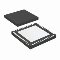
LMH0036SQX/NOPB National Semiconductor, LMH0036SQX/NOPB Datasheet - Page 8

LMH0036SQX/NOPB
Manufacturer Part Number
LMH0036SQX/NOPB
Description
IC RECLOCKER SD 4:1 MUX 48LLP
Manufacturer
National Semiconductor
Type
Reclockerr
Datasheet
1.LMH0036SQENOPB.pdf
(14 pages)
Specifications of LMH0036SQX/NOPB
Applications
SDTV/HDTV
Mounting Type
Surface Mount
Package / Case
48-LLP
Lead Free Status / RoHS Status
Lead free / RoHS Compliant
Other names
LMH0036SQX
www.national.com
SERIAL DATA CLOCK/SERIAL DATA 2 OUTPUT
The Serial Data Clock/Serial Data 2 Output is controlled by
the SCO_EN input and provides either a second retimed se-
rial data output or a low jitter differential clock output appro-
priate to the serial data rate being processed. When operating
as a serial clock output, the rising edge of the clock will be
positioned within the corresponding serial data bit interval
within 10% of the center of the data interval.
Differential output SCO/SDO2 functions as the second serial
data output when the SCO_EN input is a logic-low level. This
output functions as the serial data-rate clock output when the
SCO_EN input is a logic-high level. The SCO_EN input has
an internal pull-down device and the default state of SCO_EN
is low (serial data output 2 enabled). SCO/SDO2 is muted
when the OUTPUT MUTE input is a logic low level. When the
Bypass mode is activated and this output is functioning as a
serial clock output, the output will also be muted. If an unsup-
ported data rate is used while in Auto Bypass mode with this
output functioning as a serial clock output, the output is in-
valid.
Control Inputs and Indicator
Outputs
SERIAL DATA INPUT SELECTOR
The Serial Data Input Selector (SEL [1:0]) allows the user to
select the active input channel. Table 1 shows the input se-
lected for a given state of SEL [1:0].
SEL [1:0] Code
TABLE 1. Data Input Select Codes
00
01
10
11
FIGURE 2. Equivalent SDO Output Circuit (SDO, SDO, SCO/SDO2, SCO/SDO2)
Selected Input
SDI0
SDI1
SDI2
SDI3
8
LOCK DETECT
The Lock Detect (LD) output, when high, indicates that data
is being received and the PLL is locked. LD may be connected
to the OUTPUT MUTE input to mute the data and clock out-
puts when no data signal is being received. Note that when
the Bypass/Auto Bypass input is set high, Lock Detect will
remain low. See Table 2.
OUTPUT MUTE
The OUTPUT MUTE input, when low, mutes the serial data
and clock outputs. It may be connected to Lock Detect or ex-
ternally driven to mute or un-mute the outputs. If OUTPUT
MUTE is connected to LD, then the data and clock outputs
are muted when the PLL is not locked. This function overrides
the Bypass function: see Table 2. OUTPUT MUTE has an
internal pull-up device to enable the output by default.
BYPASS/AUTO BYPASS
The Bypass/Auto Bypass input, when high, forces the device
to output the data without reclocking it. When this input is low,
the device automatically bypasses the reclocking function
when the device is in an unlocked condition or the detected
data rate is a rate which the device does not support. Note
that when the Bypass/Auto Bypass input is set high, Lock
Detect will remain low. See Table 2. BYPASS/AUTO BY-
PASS has an internal pull-down device.
30003109


