AP40N03GS Advanced Power Electronics Corp., AP40N03GS Datasheet

Advanced Power MOSFETs from APEC provide the designer with the best combination of fast switching,ruggedized device design, low on-resistance and cost-effectiveness

AP40N03GS

Manufacturer Part Number
AP40N03GS
Description
Advanced Power MOSFETs from APEC provide the designer with the best combination of fast switching,ruggedized device design, low on-resistance and cost-effectiveness
Manufacturer
Advanced Power Electronics Corp.
Datasheet

Specifications of AP40N03GS

Vds
30V
Vgs
±20V
Rds(on) / Max(m?) Vgs@10v
17
Rds(on) / Max(m?) Vgs@4.5v
23
Qg (nc)
17
Qgs (nc)
3
Qgd (nc)
10
Id(a)
40
Pd(w)
50
Configuration
Single N
Package
TO-263
▼ Low Gate Charge
▼ Simple Drive Requirement
▼ Fast Switching Characteristic
Data & specifications subject to change without notice
V
V
I
I
I
P
T
T
Rthj-c
Rthj-a
Description
Absolute Maximum Ratings
Thermal Data
The TO-263 package is widely preferred for all commercial-industrial
surface mount applications and suited for low voltage applications
such as DC/DC converters.
D
D
DM
Advanced Power MOSFETs from APEC provide the
designer with the best combination of fast switching,
ruggedized device design, low on-resistance and cost-effectiveness.
STG
J
DS
GS
D
@T
@T
@T
C
C
Symbol
Symbol
C
=25℃
=100℃
=25℃
Advanced Power
Electronics Corp.
Drain-Source Voltage
Gate-Source Voltage
Continuous Drain Current, V
Pulsed Drain Current
Total Power Dissipation
Linear Derating Factor
Storage Temperature Range
Operating Junction Temperature Range
Maximum Thermal Resistance, Junction-case
Maximum Thermal Resistance, Junction-ambient (PCB mount)
Parameter
Parameter
1
G
GS
GS
D
@ 10V
@ 10V
S
TO-263
N-CHANNEL ENHANCEMENT MODE
POWER MOS FET
RoHS-compliant Product
3
-55 to 150
-55 to 150
Rating
BV
R
I
D
G
+20
169
0.4
30
40
30
50
DS(ON)
DSS
Value
2.5
40
AP40N03GS
D
S
200910094
17mΩ
Units
W/℃
℃/W
℃/W
30V
40A
Unit
W
V
V
A
A
A
1

Related parts for AP40N03GS

AP40N03GS Summary of contents

Page 1

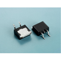
... Maximum Thermal Resistance, Junction-case Rthj-a Maximum Thermal Resistance, Junction-ambient (PCB mount) Data & specifications subject to change without notice N-CHANNEL ENHANCEMENT MODE POWER MOS FET G D TO-263 S Parameter @ 10V GS @ 10V GS 1 Parameter AP40N03GS RoHS-compliant Product BV 30V DSS R 17mΩ DS(ON) I 40A Rating Units 30 ...

Page 2

... AP40N03GS Electrical Characteristics@T Symbol Parameter BV Drain-Source Breakdown Voltage DSS Breakdown Voltage Temperature Coefficient ΔBV /ΔT DSS j R Static Drain-Source On-Resistance DS(ON) V Gate Threshold Voltage GS(th) g Forward Transconductance fs I Drain-Source Leakage Current DSS Drain-Source Leakage Current (T I Gate-Source Forward Leakage GSS Q Total Gate Charge ...

Page 3

... V Fig 2. Typical Output Characteristics 2.0 I =18A D V =10V G 1.4 0.8 0 -50 Fig 4. Normalized On-Resistance v.s. Junction Temperature 2.0 1.8 1.6 1 1.2 1.0 1 -50 Fig 6. Gate Threshold Voltage v.s. AP40N03GS o 10V C 9.0V 8.0V 7.0V 6.0V 5.0V 4.0V V =3.0V G 4.0 6.0 8.0 10.0 , Drain-to-Source Voltage ( 100 150 Junction Temperature ( 100 150 Junction Temperature ( ...

Page 4

... AP40N03GS 16 I =18A =16V DS V =20V DS V =24V Total Gate Charge (nC) G Fig 7. Gate Charge Characteristics 1000 100 Operation in this area limited by R DS(ON = Single Pulse 1 0 ,Drain-to-Source Voltage (V) DS Fig 9. Maximum Safe Operating Area ...

Related keywords