AP6679GH Advanced Power Electronics Corp., AP6679GH Datasheet - Page 2
AP6679GH
Manufacturer Part Number
AP6679GH
Description
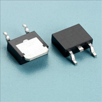
The TO-252 package is widely preferred for commercial-industrial surface mount applications and suited for low voltage applications such as DC/DC converters
Manufacturer
Advanced Power Electronics Corp.
Datasheet
1.AP6679GH.pdf
(6 pages)
Specifications of AP6679GH
Vds
-30V
Vgs
±25V
Rds(on) / Max(m?) Vgs@10v
9
Rds(on) / Max(m?) Vgs@4.5v
15
Qg (nc)
42
Qgs (nc)
6
Qgd (nc)
25
Id(a)
-75
Pd(w)
89
Configuration
Single P
Package
TO-252
Available stocks
Company
Part Number
Manufacturer
Quantity
Price
Company:

Part Number:
AP6679GH
Manufacturer:
APEC
Quantity:
9 000
Part Number:
AP6679GH
Manufacturer:
APEC/富鼎
Quantity:
20 000
Part Number:
AP6679GH-HF
Manufacturer:
APEC/富鼎
Quantity:
20 000


ΔBV
BV
R
V
g
I
I
Q
Q
Q
t
t
t
t
C
C
C
V
t
Q
1.Pulse width limited by Max. junction temperature.
2.Pulse test
3.Package limitation current is -75A .
4.Surface mounted on 1 in
THIS PRODUCT IS SENSITIVE TO ELECTROSTATIC DISCHARGE, PLEASE HANDLE WITH CAUTION.
USE OF THIS PRODUCT AS A CRITICAL COMPONENT IN LIFE SUPPORT OR OTHER SIMILAR SYSTEMS IS NOT AUTHORIZED.
APEC DOES NOT ASSUME ANY LIABILITY ARISING OUT OF THE APPLICATION OR USE OF ANY PRODUCT OR CIRCUIT DESCRIBED
HEREIN; NEITHER DOES IT CONVEY ANY LICENSE UNDER ITS PATENT RIGHTS, NOR THE RIGHTS OF OTHERS.
APEC RESERVES THE RIGHT TO MAKE CHANGES WITHOUT FURTHER NOTICE TO ANY PRODUCTS HEREIN TO IMPROVE
RELIABILITY, FUNCTION OR DESIGN.
Electrical Characteristics@T
Source-Drain Diode
Notes:
AP6679GH/J
DSS
GSS
d(on)
r
d(off)
f
rr
fs
GS(th)
SD
DS(ON)
iss
oss
rss
g
gs
gd
rr
DSS
Symbol
Symbol
DSS
/ΔT
j
Drain-Source Breakdown Voltage
Breakdown Voltage Temperature Coefficient
Static Drain-Source On-Resistance
Gate Threshold Voltage
Forward Transconductance
Drain-Source Leakage Current
Drain-Source Leakage Current (T
Gate-Source Leakage
Total Gate Charge
Gate-Source Charge
Gate-Drain ("Miller") Charge
Turn-on Delay Time
Rise Time
Turn-off Delay Time
Fall Time
Input Capacitance
Output Capacitance
Reverse Transfer Capacitance
Forward On Voltage
Reverse Recovery Time
Reverse Recovery Charge
2
copper pad of FR4 board
Parameter
Parameter
2
2
2
2
j
=25
j
=125
o
C(unless otherwise specified)
2
o
C)
V
Reference to 25℃, I
V
V
V
V
V
V
V
I
V
V
V
I
R
R
V
V
f=1.0MHz
I
I
dI/dt=-100A/µs
D
D
S
S
GS
GS
GS
DS
DS
DS
DS
GS
DS
GS
DS
GS
DS
=-16A
=-16A
G
D
=-24A, V
=-16A, V
=0.94Ω
=3.3Ω,V
=V
=-10V, I
=-30V, V
=-24V, V
=-24V
=-15V
=-25V
=0V, I
=-10V, I
=-4.5V, I
= +25V, V
=-4.5V
=0V
GS
Test Conditions
Test Conditions
, I
D
D
GS
GS
=-250uA
=-250uA
D
GS
D
D
GS
GS
=-30A
=-24A
=0V
=0V,
=-24A
DS
=-10V
=0V
=0V
=0V
D
=-1mA
Min.
Min.
-30
-1
-
-
-
-
-
-
-
-
-
-
-
-
-
-
-
-
-
-
-
-
2870 4590
-0.03
Typ.
Typ.
960
740
34
42
25
11
35
58
78
47
43
6
-
-
-
-
-
-
-
-
+100
Max. Units
Max. Units
-250
-1.2
15
67
-3
-1
9
-
-
-
-
-
-
-
-
-
-
-
-
-
V/℃
mΩ
mΩ
nC
nC
nC
nC
uA
uA
nA
pF
pF
pF
ns
ns
ns
ns
ns
V
V
S
V
2
Related parts for AP6679GH
Image
Part Number
Description
Manufacturer
Datasheet
Request
R
