AP90T03GS Advanced Power Electronics Corp., AP90T03GS Datasheet

Advanced Power MOSFETs from APEC provide the designer with the best combination of fast switching, ruggedized device design, low on-resistance and cost-effectiveness

AP90T03GS

Manufacturer Part Number
AP90T03GS
Description
Advanced Power MOSFETs from APEC provide the designer with the best combination of fast switching, ruggedized device design, low on-resistance and cost-effectiveness
Manufacturer
Advanced Power Electronics Corp.
Datasheet

Specifications of AP90T03GS

Vds
30V
Vgs
±20V
Rds(on) / Max(m?) Vgs@10v
4
Rds(on) / Max(m?) Vgs@4.5v
6
Qg (nc)
60
Qgs (nc)
8.5
Qgd (nc)
38
Id(a)
75
Pd(w)
96
Configuration
Single N
Package
TO-263
▼ Lower On- resistance
▼ Simple Drive Requirement
▼ Fast Switching Characteristic
V
V
I
I
I
P
T
T
Rthj-c
Rthj-a
Data and specifications subject to change without notice
Description
The TO-263 package is widely preferred for commercial-industrial
surface mount applications and suited for low voltage applications
such as DC/DC converters.
Absolute Maximum Ratings
Thermal Data
Advanced Power MOSFETs from APEC provide the designer with
the best combination of fast switching, ruggedized device design,
low on-resistance and cost-effectiveness.
D
D
DM
STG
J
DS
GS
D
@T
@T
@T
c
c
Symbol
Symbol
=25℃
=100℃
c
=25℃
Advanced Power
Electronics Corp.
Drain-Source Voltage
Gate-Source Voltage
Continuous Drain Current, V
Pulsed Drain Current
Total Power Dissipation
Linear Derating Factor
Storage Temperature Range
Operating Junction Temperature Range
Maximum Thermal Resistance, Junction-case
Maximum Thermal Resistance, Junction-ambient
Parameter
Parameter
1
GS
GS
G
@10V
@10V
3
D
S
N-CHANNEL ENHANCEMENT MODE
POWER MOSFET
RoHS-compliant Product
-55 to 150
-55 to 150
Rating
BV
R
I
D
G
±20
350
0.7
30
75
63
96
DS(ON)
DSS
D
Value
1.3
62
S
AP90T03GS
TO-263(S)
200802183
4mΩ
Units
W/℃
Units
℃/W
℃/W
30V
75A
W
V
V
A
A
A
1

Related parts for AP90T03GS

AP90T03GS Summary of contents

Page 1

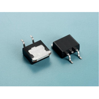
... Maximum Thermal Resistance, Junction-case Rthj-a Maximum Thermal Resistance, Junction-ambient Data and specifications subject to change without notice RoHS-compliant Product N-CHANNEL ENHANCEMENT MODE POWER MOSFET Parameter 3 @10V GS @10V GS 1 Parameter AP90T03GS BV 30V DSS R 4mΩ DS(ON) I 75A TO-263(S) S Rating Units 30 V ±20 ...

Page 2

... AP90T03GS Electrical Characteristics@T Symbol Parameter BV Drain-Source Breakdown Voltage DSS R Static Drain-Source On-Resistance DS(ON) V Gate Threshold Voltage GS(th) g Forward Transconductance fs I Drain-Source Leakage Current DSS Drain-Source Leakage Current (T I Gate-Source Leakage GSS Q Total Gate Charge g Q Gate-Source Charge gs Q Gate-Drain ("Miller") Charge gd t Turn-on Delay Time ...

Page 3

... Fig 2. Typical Output Characteristics 2 1.8 1.5 1.3 1.0 0.8 0.5 0.3 0.0 10 -50 Fig 4. Normalized On-Resistance v.s. Junction Temperature 0.5 0 -50 0.8 0 Fig 6. Gate Threshold Voltage v.s. AP90T03GS o 10V 7.0V 5.0V 4.5V V =3. Drain-to-Source Voltage ( 100 Junction Temperature ( 100 o , Junction Temperature ( C) j Junction Temperature 5 150 ...

Page 4

... AP90T03GS =15V DS V =20V =24V Total Gate Charge (nC) G Fig 7. Gate Charge Characteristics 1000 100 = Single 1 0 ,Drain-to-Source Voltage (V) DS Fig 9. Maximum Safe Operating Area V DS 90% 10 ...

Page 5

... ADVANCED POWER ELECTRONICS CORP. Package Outline : TO-263 Part Marking Information & Packing : TO-263 XXXXXS 90T03GS YWWSSS YWWSSS θ θ Part Number Part Number Package Code Package Code LOGO ...

Related keywords