AP9T18GEH Advanced Power Electronics Corp., AP9T18GEH Datasheet

The Advanced Power MOSFETs from APEC provide the designer with the best combination of fast switching, ruggedized device design, ultra low on-resistance and cost-effectiveness

AP9T18GEH

Manufacturer Part Number
AP9T18GEH
Description
The Advanced Power MOSFETs from APEC provide the designer with the best combination of fast switching, ruggedized device design, ultra low on-resistance and cost-effectiveness
Manufacturer
Advanced Power Electronics Corp.
Datasheet

Specifications of AP9T18GEH

Vds
20V
Vgs
±12V
Rds(on) / Max(m?) Vgs@4.5v
14
Rds(on) / Max(m?) Vgs@2.5v
28
Qg (nc)
16
Qgs (nc)
2
Qgd (nc)
6
Id(a)
40
Pd(w)
31
Configuration
Single N
Package
TO-252
▼ G-S Diode embedded
▼ Capable of 2.5V gate drive
▼ Surface mount package
▼ RoHS Compliant
The Advanced Power MOSFETs from APEC provide the
designer with the best combination of fast switching,
ruggedized device design, ultra low on-resistance and
cost-effectiveness.
V
V
I
I
I
P
T
T
Rthj-c
Rthj-a
Data and specifications subject to change without notice
Description
Absolute Maximum Ratings
Thermal Data
D
D
DM
STG
J
DS
GS
D
@T
@T
@T
C
C
Symbol
Symbol
C
=25℃
=100℃
=25℃
Advanced Power
Electronics Corp.
Thermal Resistance Junction-case
Thermal Resistance Junction-ambient
Drain-Source Voltage
Gate-Source Voltage
Continuous Drain Current, V
Pulsed Drain Current
Total Power Dissipation
Linear Derating Factor
Storage Temperature Range
Operating Junction Temperature Range
Parameter
Parameter
1
GS
GS
@ 4.5V
@ 4.5V
G
N-CHANNEL ENHANCEMENT MODE
POWER MOSFET
D
S
Max.
Max.
Pb Free Plating Product
-55 to 150
-55 to 150
Rating
BV
R
I
D
0.25
±12
160
20
40
25
31
DS(ON)
G
G
DSS
D
AP9T18GEH/J
Value
S
D S
110
4
TO-252(H)
TO-251(J)
200523061-1/4
14mΩ
Units
Units
W/℃
℃/W
℃/W
20V
40A
W
V
V
A
A
A

Related parts for AP9T18GEH

AP9T18GEH Summary of contents

Page 1

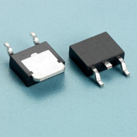
... Operating Junction Temperature Range J Thermal Data Symbol Rthj-c Thermal Resistance Junction-case Rthj-a Thermal Resistance Junction-ambient Data and specifications subject to change without notice N-CHANNEL ENHANCEMENT MODE POWER MOSFET G Parameter @ 4. 4. Parameter AP9T18GEH/J Pb Free Plating Product BV 20V D DSS R 14mΩ DS(ON) I 40A TO-252( TO-251(J) ...

Page 2

... AP9T18GEH/J Electrical Characteristics@T Symbol Parameter BV Drain-Source Breakdown Voltage DSS ΔBV Breakdown Voltage Temperature Coefficient /ΔT DSS j R Static Drain-Source On-Resistance DS(ON) V Gate Threshold Voltage GS(th) g Forward Transconductance fs I Drain-Source Leakage Current (T DSS Drain-Source Leakage Current (T I Gate-Source Leakage GSS Q Total Gate Charge g Q Gate-Source Charge ...

Page 3

... Fig 2. Typical Output Characteristics 1.6 I =20A D V =4. 1.4 1.2 1.0 0.8 0 Fig 4. Normalized On-Resistance v.s. Junction Temperature 40 20.0 10.0 0 Fig 6. On-Resistance vs. Drain Current AP9T18GEH 150 C C 4.5V 3.5V 2.5V V =1. Drain-to-Source Voltage ( 100 125 150 o , Junction Temperature ( =2. =4. ...

Page 4

... AP9T18GEH =20A =10V DS V =12V =16V Total Gate Charge (nC) G Fig 7. Gate Charge Characteristics 1000 100 Drain-to-Source Voltage (V) DS Fig 9. Maximum Safe Operating Area ...

Related keywords