AP97T07GW-HF Advanced Power Electronics Corp., AP97T07GW-HF Datasheet
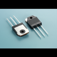
AP97T07GW-HF

Manufacturer Part Number
AP97T07GW-HF
Description
Manufacturer
Advanced Power Electronics Corp.
Datasheet

Specifications of AP97T07GW-HF

Vds
75V
Vgs
±20V
Rds(on) / Max(m?) Vgs@10v
3.6
Qg (nc)
110
Qgs (nc)
15
Qgd (nc)
60
Id(a)
220
Pd(w)
375
Configuration
Single N
Package
TO-3P
▼ Simple Drive Requirement
▼ Lower On-resistance
▼ RoHS Compliant & Halogen-Free
V
V
I
I
I
I
P
T
T
Rthj-c
Rthj-a
Data and specifications subject to change without notice
Description
Absolute Maximum Ratings
Thermal Data
Advanced Power MOSFETs from APEC provide the
designer with the best combination of fast switching,
ruggedized device design, low on-resistance and cost-effectiveness.
The TO-3P package is widely preferred for commercial-industrial
surface mount applications and suited for higher voltage applications
such as SMPS.
D
D
D
DM
STG
J
DS
GS
D
@T
@T
@T
@T
C
C
C
Symbol
Symbol
C
=25℃
=25℃
=100℃
=25℃
Advanced Power
Electronics Corp.
Drain-Source Voltage
Gate-Source Voltage
Continuous Drain Current (Chip)
Continuous Drain Current, V
Pulsed Drain Current
Total Power Dissipation
Storage Temperature Range
Operating Junction Temperature Range
Maximum Thermal Resistance, Junction-case
Maixmum Thermal Resistance, Junction-ambient
Parameter
Parameter
1
GS
GS
G
@ 10V
@ 10V
3
3
D
S
N-CHANNEL ENHANCEMENT MODE
POWER MOSFET
Halogen-Free Product
-55 to 175
-55 to 175
G
Rating
BV
R
I
D
D
+20
220
120
120
480
375
AP97T07GW-HF
75
DS(ON)
DSS
S
Value
0.4
40
TO-3P
3.6mΩ
201012281
220A
Units
Units
℃/W
℃/W
75V
W
V
V
A
A
A
A
1

Related parts for AP97T07GW-HF

AP97T07GW-HF Summary of contents

Page 1

... Rthj-c Maximum Thermal Resistance, Junction-case Rthj-a Maixmum Thermal Resistance, Junction-ambient Data and specifications subject to change without notice N-CHANNEL ENHANCEMENT MODE POWER MOSFET Parameter 3 @ 10V 10V GS 1 Parameter AP97T07GW-HF Halogen-Free Product BV 75V DSS R 3.6mΩ DS(ON) I 220A D G TO- Rating Units 75 V +20 ...

Page 2

... AP97T07GW-HF Electrical Characteristics@T Symbol Parameter BV Drain-Source Breakdown Voltage DSS R Static Drain-Source On-Resistance DS(ON) V Gate Threshold Voltage GS(th) g Forward Transconductance fs I Drain-Source Leakage Current DSS I Gate-Source Leakage GSS Q Total Gate Charge g Q Gate-Source Charge gs Q Gate-Drain ("Miller") Charge gd t Turn-on Delay Time d(on) t Rise Time ...

Page 3

... D V =10V G 2.2 1.8 1.4 1.0 0.6 0.2 - Fig 4. Normalized On-Resistance v.s. Junction Temperature 1.6 I =1mA D 1 0.8 0.4 0.0 1.2 1.4 -50 0 Fig 6. Gate Threshold Voltage v.s. Junction Temperature AP97T07GW- 175 C C 10V 8.0V 7.0V 6.0V V =5. Drain-to-Source Voltage ( 100 150 200 Junction Temperature ( 100 150 200 o ...

Page 4

... AP97T07GW- =40V =45V DS V =60V Total Gate Charge (nC) G Fig 7. Gate Charge Characteristics 1000 Operation in this area limited by R DS(ON) 100 = Single Pulse 1 0 Drain-to-Source Voltage (V) DS Fig 9. Maximum Safe Operating Area ...

Related keywords