CD4050BCM Fairchild Semiconductor, CD4050BCM Datasheet
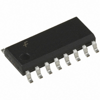
IC BUFFER HEX NON-INV 16SOIC

CD4050BCM

Manufacturer Part Number
CD4050BCM
Description
IC BUFFER HEX NON-INV 16SOIC
Manufacturer
Fairchild Semiconductor
Series
4000Br
Datasheet

Specifications of CD4050BCM

Logic Type
Buffer, Hex Converter
Number Of Elements
6
Number Of Bits Per Element
1
Current - Output High, Low
12mA, 40mA
Voltage - Supply
3 V ~ 15 V
Operating Temperature
-55°C ~ 125°C
Mounting Type
Surface Mount
Package / Case
16-SOIC (3.9mm Width)
Logic Family
CD40
Number Of Channels Per Chip
Hex
Polarity
Non-Inverting
Supply Voltage (max)
15 V
Supply Voltage (min)
3 V
Maximum Operating Temperature
125 C
Mounting Style
SMD/SMT
High Level Output Current
- 8 mA (Min)
Input Bias Current (max)
4 uA
Low Level Output Current
35 mA (Min)
Maximum Power Dissipation
500 mW
Minimum Operating Temperature
- 55 C
Propagation Delay Time
85 ns @ 5 V or 45 ns @ 10 V or 35 ns @ 15 V
Lead Free Status / RoHS Status
Lead free / RoHS Compliant

Available stocks

Company
Part Number
Manufacturer
Quantity
Price
Part Number:
CD4050BCMX
Manufacturer:
FSC
Quantity:
696
© 1999 Fairchild Semiconductor Corporation
CD4049UBCM
CD4049UBCN
CD4050BCM
CD4050BCN
CD4049UBC • CD4050BC
Hex Inverting Buffer •
Hex Non-Inverting Buffer
General Description
The CD4049UBC and CD4050BC hex buffers are mono-
lithic complementary MOS (CMOS) integrated circuits con-
structed with N- and P-channel enhancement mode
transistors. These devices feature logic level conversion
using only one supply voltage (V
level (V
devices are used for logic level conversions. These
devices are intended for use as hex buffers, CMOS to DTL/
TTL converters, or as CMOS current drivers, and at V
5.0V, they can drive directly two DTL/TTL loads over the
full operating temperature range.
Ordering Code:
Devices also available in Tape and Reel. Specify by appending the suffix letter “X” to the ordering code.
Connection Diagrams
Order Number
IH
) can exceed the V
Package Number
CD4049UBC
Top View
M16A
M16A
N16E
N16E
DD
supply voltage when these
DD
). The input signal high
16-Lead Small Outline Integrated Circuit (SOIC), JEDEC MS-012, 0.150” Narrow
16-Lead Plastic Dual-In-Line Package (PDIP), JEDEC MS-001, 0.300” Wide
16-Lead Small Outline Integrated Circuit (SOIC), JEDEC MS-012, 0.150” Narrow
16-Lead Plastic Dual-In-Line Package (PDIP), JEDEC MS-001, 0.300” Wide
DS005971.prf
Pin Assignments for DIP
DD
Features
Applications
• CMOS hex inverter/buffer
• CMOS to DTL/TTL hex converter
• CMOS current “sink” or “source” driver
• CMOS HIGH-to-LOW logic level converter
Wide supply voltage range:
Direct drive to 2 TTL loads at 5.0V over full temperature
range
High source and sink current capability
Special input protection permits input voltages greater
than V
Package Description
DD
CD4050BC
Top View
October 1987
Revised January 1999
3.0V to 15V
www.fairchildsemi.com

Related parts for CD4050BCM

CD4050BCM Summary of contents

Page 1

... M16A 16-Lead Small Outline Integrated Circuit (SOIC), JEDEC MS-012, 0.150” Narrow CD4049UBCN N16E 16-Lead Plastic Dual-In-Line Package (PDIP), JEDEC MS-001, 0.300” Wide CD4050BCM M16A 16-Lead Small Outline Integrated Circuit (SOIC), JEDEC MS-012, 0.150” Narrow CD4050BCN N16E 16-Lead Plastic Dual-In-Line Package (PDIP), JEDEC MS-001, 0.300” Wide Devices also available in Tape and Reel. Specify by appending the suffix letter “ ...

Page 2

Schematic Diagrams www.fairchildsemi.com CD4049UBC Identical Units CD4050BC Identical Units 2 ...

Page 3

Absolute Maximum Ratings (Note 2) Supply Voltage ( Input Voltage ( Voltage at Any Output Pin ( OUT Storage Temperature Range ( Power Dissipation ( Dual-In-Line Small Outline ...

Page 4

DC Electrical Characteristics Note 4: These are peak output current capabilities. Continuous output current is rated maximum. The output current should not be allowed to exceed this value for extended periods of time. I and I OL ...

Page 5

Switching Time Waveforms Typical Applications CMOS to TLL or CMOS at a Lower DD1 DD2 In the case of the CD4049UBC the output drive capability increases with increasing input voltage. E.g 10V the CD4049UBC could ...

Page 6

Physical Dimensions inches (millimeters) unless otherwise noted 16-Lead Small Outline Integrated Circuit (SOIC), JEDEC MS-012, 0.150” Narrow www.fairchildsemi.com Package Number M16A 6 ...

Page 7

Physical Dimensions inches (millimeters) unless otherwise noted (Continued) 16-Lead Plastic Dual-In-Line Package (PDIP), JEDEC MS-001, 0.300” Wide LIFE SUPPORT POLICY FAIRCHILD’S PRODUCTS ARE NOT AUTHORIZED FOR USE AS CRITICAL COMPONENTS IN LIFE SUPPORT DEVICES OR SYSTEMS WITHOUT THE EXPRESS WRITTEN ...

Related keywords