DM74ALS125M Fairchild Semiconductor, DM74ALS125M Datasheet

IC BUFF TRI-ST QD N-INV 14SOIC

DM74ALS125M

Manufacturer Part Number
DM74ALS125M
Description
IC BUFF TRI-ST QD N-INV 14SOIC
Manufacturer
Fairchild Semiconductor
Series
74ALSr
Datasheet

Specifications of DM74ALS125M

Logic Type
Buffer/Line Driver, Non-Inverting
Number Of Elements
4
Number Of Bits Per Element
1
Current - Output High, Low
15mA, 24mA
Voltage - Supply
4.5 V ~ 5.5 V
Operating Temperature
0°C ~ 70°C
Mounting Type
Surface Mount
Package / Case
14-SOIC (3.9mm Width), 14-SOL
Dc
0418
Lead Free Status / RoHS Status
Lead free / RoHS Compliant
© 2000 Fairchild Semiconductor Corporation
DM74ALS125M
DM74ALS125N
DM74ALS125
Quad 3-STATE Buffer
General Description
This device contains four independent gates each of which
performs a non-inverting buffer function. The outputs have
the 3-STATE feature. The 3-STATE circuitry contains a fea-
ture that maintains the buffer outputs in 3-STATE (high
impedance state) during power supply ramp-up or ramp-
down. This eliminates bus glitching problems that arise
during power-up and power-down. To minimize the possi-
bility that two outputs will attempt to take a common bus to
opposite logic levels, the disable time is shorter than the
enable time of the outputs.
Ordering Code:
Devices also available in Tape and Reel. Specify by appending the suffix letter “X” to the ordering code.
Connection Diagram
Functional Table
H
L
X
Hi-Z
Order Number
LOW Logic Level
HIGH Logic Level
Either LOW or HIGH Logic Level
3-STATE (Outputs are disabled)
A
H
X
L
Package Number
Input
M14A
N14A
Y
C
H
L
L
A
Output
14-Lead Small Outline Integrated Circuit (SOIC), JEDEC MS-012, 0.150 Narrow
14-Lead Plastic Dual-In-Line Package (PDIP), JEDEC MS-001, 0.300 Wide
Hi-Z
Y
H
L
DS010620
Features
Logic Diagram
Advanced low power oxide-isolated ion-implanted
Schottky TTL process
Functional and pin compatible with the 74LS counterpart
Switching response specified into 500 and 50 pF load
Switching response specifications guaranteed over full
temperature and V
PNP input design reduces input loading
Low level drive current: 74ALS
Package Description
CC
supply range
November 1989
Revised February 2000
24 mA
www.fairchildsemi.com

Related parts for DM74ALS125M

DM74ALS125M Summary of contents

Page 1

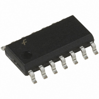
... Ordering Code: Order Number Package Number DM74ALS125M M14A 14-Lead Small Outline Integrated Circuit (SOIC), JEDEC MS-012, 0.150 Narrow DM74ALS125N N14A 14-Lead Plastic Dual-In-Line Package (PDIP), JEDEC MS-001, 0.300 Wide Devices also available in Tape and Reel. Specify by appending the suffix letter “ ...

Page 2

Absolute Maximum Ratings Supply Voltage Input Voltage Voltage Applied to Disabled Output Operating Free Air Temperature Range Storage Temperature Range Typical JA N Package M Package Recommended Operating Conditions Symbol Parameter V Supply Voltage CC V HIGH Level ...

Page 3

Switching Characteristics Symbol Parameter t Propagation Delay Time PLH LOW-to-HIGH Level Output t Propagation Delay Time PHL HIGH-to-LOW Level Output t Output Enable Time PZH to HIGH Level Output t Output Enable Time PZL to LOW Level Output t Output ...

Page 4

Physical Dimensions inches (millimeters) unless otherwise noted 14-Lead Small Outline Integrated Circuit (SOIC), JEDEC MS-012, 0.150 Narrow www.fairchildsemi.com Package Number M14A 4 ...

Page 5

Physical Dimensions inches (millimeters) unless otherwise noted (Continued) 14-Lead Plastic Dual-In-Line Package (PDIP), JEDEC MS-001, 0.300 Wide Fairchild does not assume any responsibility for use of any circuitry described, no circuit patent licenses are implied and Fairchild reserves the right ...

Related keywords