74ABT646ADB,112 NXP Semiconductors, 74ABT646ADB,112 Datasheet - Page 8
74ABT646ADB,112
Manufacturer Part Number
74ABT646ADB,112
Description
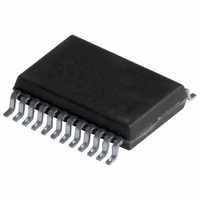
IC TRANSCVR 8BIT N-INV 24SSOP
Manufacturer
NXP Semiconductors
Series
74ABTr
Datasheet
1.74ABT646ADB118.pdf
(19 pages)
Specifications of 74ABT646ADB,112
Logic Type
Registered Transceiver, Non-Inverting
Package / Case
24-SSOP
Number Of Elements
1
Number Of Bits Per Element
8
Current - Output High, Low
32mA, 64mA
Voltage - Supply
4.5 V ~ 5.5 V
Operating Temperature
-40°C ~ 85°C
Mounting Type
Surface Mount
Logic Family
ABT
Number Of Channels Per Chip
8
Input Level
TTL
Output Level
TTL
Output Type
3-State
High Level Output Current
- 32 mA
Low Level Output Current
64 mA
Propagation Delay Time
5.2 ns
Supply Voltage (max)
5.5 V
Supply Voltage (min)
4.5 V
Maximum Operating Temperature
+ 85 C
Function
Bus Transceiver / Register
Input Bias Current (max)
30000 uA
Minimum Operating Temperature
- 40 C
Mounting Style
SMD/SMT
Polarity
Non-Inverting
Number Of Circuits
1
Lead Free Status / RoHS Status
Lead free / RoHS Compliant
Lead Free Status / RoHS Status
Lead free / RoHS Compliant, Lead free / RoHS Compliant
Other names
74ABT646ADB
74ABT646ADB
935192640112
74ABT646ADB
935192640112


NXP Semiconductors
9. Static characteristics
Table 6.
[1]
[2]
[3]
[4]
[5]
74ABT646A_3
Product data sheet
Symbol Parameter
V
V
V
V
I
I
I
I
I
I
I
C
C
I
OFF
O(pu/pd)
OZ
LO
O
CC
I
IK
OH
OL
OL(pu)
I
I/O
CC
For valid test results, data must not be loaded into the flip-flops (or latches) after applying the power.
This parameter is valid for any V
transition time of up to 100 s is permitted.
Not more than one output should be tested at a time, and the duration of the test should not exceed one second.
This is the increase in supply current for each input at 3.4 V.
This data sheet limit may vary among suppliers.
input clamping voltage
HIGH-level output
voltage
LOW-level output voltage V
power-up LOW-level
output voltage
input leakage current
power-off leakage current V
power-up/power-down
output current
OFF-state output current V
output leakage current
output current
supply current
additional supply current
input capacitance
input/output capacitance
Static characteristics
CC
between 0 V and 2.1 V with a transition time of up to 10 ms. For V
Conditions
V
V
V
V
V
V
V
V
V
V
V
V
V
per input pin; V
at 3.4 V; other inputs at V
control pins; V
I/O pins; outputs disabled; V
or V
CC
I
CC
I
CC
I
CC
CC
CC
I
CC
CC
O
I
CC
CC
V
V
V
control pins
data pins
V
V
outputs HIGH-state
outputs LOW-state
outputs disabled
= V
= V
= GND or V
= GND or V
= GND or V
= 5.5 V; V
CC
CC
CC
O
O
CC
= 4.5 V; I
= 4.5 V; I
= 5.5 V; I
= 5.5 V; V
= 0 V; V
= 2.1 V; V
= 5.5 V; V
= 5.5 V; HIGH-state;
= 5.5 V; V
= 5.5 V; V
All information provided in this document is subject to legal disclaimers.
= 2.7 V
= 0.5 V
IL
IL
= 4.5 V; I
= 5.0 V; I
= 4.5 V; I
or V
or V
IH
IH
I
Rev. 03 — 15 March 2010
CC
IK
OL
O
or V
CC
CC
CC
I
I
O
I
O
I
CC
= 0 V or V
= 1 mA;
= GND or 5.5 V
= V
= GND or V
= 18 mA
OH
OH
OH
= 0.5 V;
= 5.5 V;
= 2.5 V
= 64 mA;
; OE HIGH
O
= 5.5 V; one input
= 3 mA
= 3 mA
= 32 mA
IL
or V
4.5 V
IH
CC
CC
CC
O
or GND
= 0 V
[3][5]
[1]
[2]
[4]
Octal bus transceiver/register; 3-state
Min
2.5
3.0
2.0
180
1.2
-
-
-
-
-
-
-
-
-
-
-
-
-
-
-
25 C
0.13 0.55
Typ
110
110
3.0
3.5
2.4
0.3
5.0
5.0
0.6
20
0.9
0.0
5.0
5.0
5.0
1
65
4
7
5
CC
Max
0.55
250
250
1.5
100
100
50
50
30
1.0
50
50
40
-
-
-
-
-
-
74ABT646A
= 2.1 V to V
40 C to 85 C Unit
Min
2.5
3.0
2.0
180
1.2
© NXP B.V. 2010. All rights reserved.
-
-
-
-
-
-
-
-
-
-
-
-
-
-
-
CC
= 5 V
Max
0.55
0.55
250
250
1.5
100
100
50
50
30
1.0
50
50
40
-
-
-
-
-
-
10 %, a
8 of 19
V
V
V
V
V
V
mA
mA
mA
pF
pF
A
A
A
A
A
A
A
A
A
Related parts for 74ABT646ADB,112
Image
Part Number
Description
Manufacturer
Datasheet
Request
R

Part Number:
Description:
NXP Semiconductors designed the LPC2420/2460 microcontroller around a 16-bit/32-bitARM7TDMI-S CPU core with real-time debug interfaces that include both JTAG andembedded trace
Manufacturer:
NXP Semiconductors
Datasheet:

Part Number:
Description:
NXP Semiconductors designed the LPC2458 microcontroller around a 16-bit/32-bitARM7TDMI-S CPU core with real-time debug interfaces that include both JTAG andembedded trace
Manufacturer:
NXP Semiconductors
Datasheet:
Part Number:
Description:
NXP Semiconductors designed the LPC2468 microcontroller around a 16-bit/32-bitARM7TDMI-S CPU core with real-time debug interfaces that include both JTAG andembedded trace
Manufacturer:
NXP Semiconductors
Datasheet:
Part Number:
Description:
NXP Semiconductors designed the LPC2470 microcontroller, powered by theARM7TDMI-S core, to be a highly integrated microcontroller for a wide range ofapplications that require advanced communications and high quality graphic displays
Manufacturer:
NXP Semiconductors
Datasheet:
Part Number:
Description:
NXP Semiconductors designed the LPC2478 microcontroller, powered by theARM7TDMI-S core, to be a highly integrated microcontroller for a wide range ofapplications that require advanced communications and high quality graphic displays
Manufacturer:
NXP Semiconductors
Datasheet:
Part Number:
Description:
The Philips Semiconductors XA (eXtended Architecture) family of 16-bit single-chip microcontrollers is powerful enough to easily handle the requirements of high performance embedded applications, yet inexpensive enough to compete in the market for hi
Manufacturer:
NXP Semiconductors
Datasheet:
Part Number:
Description:
The XA-S3 device is a member of Philips Semiconductors? XA(eXtended Architecture) family of high performance 16-bitsingle-chip microcontrollers
Manufacturer:
NXP Semiconductors
Datasheet:

Part Number:
Description:
The NXP BlueStreak LH75401/LH75411 family consists of two low-cost 16/32-bit System-on-Chip (SoC) devices
Manufacturer:
NXP Semiconductors
Datasheet:
Part Number:
Description:
The NXP LPC3130/3131 combine an 180 MHz ARM926EJ-S CPU core, high-speed USB2
Manufacturer:
NXP Semiconductors
Datasheet:
Part Number:
Description:
The NXP LPC3141 combine a 270 MHz ARM926EJ-S CPU core, High-speed USB 2
Manufacturer:
NXP Semiconductors
Part Number:
Description:
The NXP LPC3143 combine a 270 MHz ARM926EJ-S CPU core, High-speed USB 2
Manufacturer:
NXP Semiconductors

Part Number:
Description:
The NXP LPC3152 combines an 180 MHz ARM926EJ-S CPU core, High-speed USB 2
Manufacturer:
NXP Semiconductors
Part Number:
Description:
The NXP LPC3154 combines an 180 MHz ARM926EJ-S CPU core, High-speed USB 2
Manufacturer:
NXP Semiconductors

Part Number:
Description:
Standard level N-channel enhancement mode Field-Effect Transistor (FET) in a plastic package using NXP High-Performance Automotive (HPA) TrenchMOS technology
Manufacturer:
NXP Semiconductors
Datasheet: