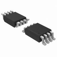
NL27WZ126USG ON Semiconductor, NL27WZ126USG Datasheet - Page 4

NL27WZ126USG
Manufacturer Part Number
NL27WZ126USG
Description
IC BUFFER DL TRI-ST NON-INV US8
Manufacturer
ON Semiconductor
Series
27WZr
Datasheet
1.NL27WZ126USG.pdf
(6 pages)
Specifications of NL27WZ126USG
Logic Type
Buffer/Line Driver, Non-Inverting
Number Of Elements
2
Number Of Bits Per Element
1
Current - Output High, Low
32mA, 32mA
Voltage - Supply
1.65 V ~ 5.5 V
Operating Temperature
-40°C ~ 85°C
Mounting Type
Surface Mount
Package / Case
US8, 8-VSSOP
Logic Family
LCX
Number Of Channels Per Chip
2
Polarity
Non-Inverting
Supply Voltage (max)
5.5 V
Supply Voltage (min)
1.65 V
Maximum Operating Temperature
+ 85 C
Mounting Style
SMD/SMT
High Level Output Current
- 32 mA
Low Level Output Current
32 mA
Maximum Power Dissipation
250 mW
Minimum Operating Temperature
- 40 C
Number Of Lines (input / Output)
2 / 3
Output Type
3-State
Propagation Delay Time
5.7 ns at 3.3 V, 5 ns at 5 V
Logic Device Type
Buffer, Non Inverting
Supply Voltage Range
1.65V To 5.5V
Logic Case Style
US8
No. Of Pins
8
Operating Temperature Range
-40°C To +85°C
Filter Terminals
SMD
Rohs Compliant
Yes
Family Type
27WZ
Lead Free Status / RoHS Status
Lead free / RoHS Compliant
Other names
NL27WZ126USGOS
NL27WZ126USGOS
NL27WZ126USGOSTR
NL27WZ126USGOS
NL27WZ126USGOSTR
Available stocks
Company
Part Number
Manufacturer
Quantity
Price
Part Number:
NL27WZ126USG
Manufacturer:
ON/安森美
Quantity:
20 000
7. C
CAPACITIVE CHARACTERISTICS
Symbol
t
OUTPUT Y
f
INPUT
A and B
C
C
Average operating current can be obtained by the equation: I
power consumption; P
= 3 ns
C
OUT
PD
PD
IN
is defined as the value of the internal equivalent capacitance which is calculated from the operating current consumption without load.
Input Capacitance
Output Capacitance
Power Dissipation Capacitance
(Note 7)
Figure 3. Switching Waveform
t
PHL
10%
V
mi
90%
V
mo
D
= C
90%
PD
V
OE
Parameter
mi
On
On
V
V
CC
t
mo
PLH
Figure 5. AC Output Enable and Disable Waveform
t
2
t
PZH
PZL
10%
f
in
t
f
= 3 ns
+ I
CC
V
V
mi
V
GND
V
V
CC
CC
OH
OL
.
http://onsemi.com
V
V
NL27WZ126
mo
mo
CC(OPR
V
V
10 MHz, V
10 MHz, V
t
t
PHZ
PLZ
CC
CC
4
)
= C
= 5.5 V, V
= 5.5 V, V
PD
INPUT
CC
CC
V
CC
= 3.3 V, V
= 5.5 V, V
V
*Includes all probe and jig capacitance.
I
I
A 1 MHz square input wave is recommended for
mi
= 0 V or V
= 0 V or V
f
in
Condition
+ I
CC
I
I
OE = GND
= 0 V or V
= 0 V or V
CC
CC
. C
Figure 4. t
propagation delay tests.
V
V
PD
V
OH
GND
CC
OL
≈ 0 V
≈ 3.0 V
is used to determine the no−load dynamic
2.7 V
0 V
− 0.3 V
+ 0.3 V
CC
CC
PLH
C
L
or t
*
PHL
Typical
R
L
2.5
2.5
11
9
OUTPUT
Unit
pF
pF
pF


