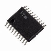
74ABT620DB,112 NXP Semiconductors, 74ABT620DB,112 Datasheet - Page 2

74ABT620DB,112
Manufacturer Part Number
74ABT620DB,112
Description
IC TRANSCEIVER 3ST 8BIT 20SSOP
Manufacturer
NXP Semiconductors
Series
74ABTr
Datasheet
1.74ABT620D602.pdf
(11 pages)
Specifications of 74ABT620DB,112
Logic Type
Transceiver, Inverting
Number Of Elements
1
Number Of Bits Per Element
8
Current - Output High, Low
32mA, 64mA
Voltage - Supply
4.5 V ~ 5.5 V
Operating Temperature
-40°C ~ 85°C
Mounting Type
Surface Mount
Package / Case
20-SSOP
Lead Free Status / RoHS Status
Lead free / RoHS Compliant
Other names
74ABT620DB
74ABT620DB
935066530112
74ABT620DB
935066530112
FEATURES
QUICK REFERENCE DATA
ORDERING INFORMATION
PIN CONFIGURATION
Philips Semiconductors
20-Pin Plastic DIP
20-Pin plastic SO
20-Pin Plastic SSOP Type II
20-Pin Plastic TSSOP Type I
1993 Jun 21
Octal bidirectional bus interface
3-State buffers
Power-up 3-State
Live insertion/extraction permitted
Output capability: +64mA/–32mA
Latch-up protection exceeds 500mA per Jedec Std 17
ESD protection exceeds 2000 V per MIL STD 883 Method 3015
and 200 V per Machine Model
Octal transceiver with dual enable, inverting
(3-State)
SYMBOL
I
t
t
C
C
PLH
PHL
CCZ
I/O
IN
PACKAGES
OEAB
GND
Propagation delay
An to Bn or Bn to An
Input capacitance
OEAB, OEBA
I/O capacitance
Total supply current
A0
A1
A2
A3
A4
A5
A6
A7
10
1
2
3
4
5
6
7
8
9
PARAMETER
TEMPERATURE RANGE
20
19
18
17
16
15
14
13
12
11
V
OEBA
B0
B1
B2
B3
B4
B5
B6
B7
–40 C to +85 C
–40 C to +85 C
–40 C to +85 C
–40 C to +85 C
CC
C
V
Outputs disabled; V
Outputs disabled; V
SA00189
L
I
= 0V or V
= 50pF; V
OUTSIDE NORTH AMERICA
2
CC
T
CC
amb
DESCRIPTION
The 74ABT620 high-performance BiCMOS device combines low
static and dynamic power dissipation with high speed and high
output drive.
The 74ABT620 device is an octal transceiver featuring inverting
3-State bus compatible outputs in both send and receive directions.
The 74ABT620 is designed for asynchronous two-way
communication between data buses. The control function
implementation allows for maximum flexibility in timing. This device
allows data transmission from the A bus to the B bus or from the B
bus to the A bus, depending upon the logic levels at the Enable
inputs (OEBA and OEAB). The Enable inputs can be used to disable
the device so that the buses are effectively isolated.
PIN DESCRIPTION
74ABT620 PW
= 5V
74ABT620 DB
74ABT620 N
74ABT620 D
PIN NUMBER
18, 17, 16, 15,
14, 13, 12, 11
CONDITIONS
= 25 C; GND = 0V
O
CC
2, 3, 4, 5,
6, 7, 8, 9
= 0V or V
= 5.5V
19
10
20
1
CC
SYMBOL
A0 – A7
B0 – B7
OEAB
OEBA
GND
V
CC
NORTH AMERICA
74ABT620PW DH
74ABT620 DB
74ABT620 N
74ABT620 D
Output enable input, A side to B side
(active-High)
Data inputs/outputs (A side)
Data inputs/outputs (B side)
Output enable input, B side to A side
(active-Low)
Ground (0V)
Positive supply voltage
NAME AND FUNCTION
TYPICAL
3.1
50
4
7
Product specification
74ABT620
DWG NUMBER
853–1611 10081
SOT146-1
SOT163-1
SOT339-1
SOT360-1
UNIT
pF
pF
ns
A


