NL27WZ17DFT2 ON Semiconductor, NL27WZ17DFT2 Datasheet
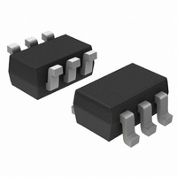
IC BUFF SCHM TRG DL N-INV SOT363

NL27WZ17DFT2

Manufacturer Part Number
NL27WZ17DFT2
Description
IC BUFF SCHM TRG DL N-INV SOT363
Manufacturer
ON Semiconductor
Series
27WZr
Datasheet

Specifications of NL27WZ17DFT2

Logic Type
Schmitt Trigger - Buffer, Driver
Number Of Elements
2
Number Of Bits Per Element
1
Current - Output High, Low
32mA, 32mA
Voltage - Supply
1.65 V ~ 5.5 V
Operating Temperature
-55°C ~ 125°C
Mounting Type
Surface Mount
Package / Case
SC-70-6, SC-88, SOT-363
Lead Free Status / RoHS Status
Contains lead / RoHS non-compliant
Other names
NL27WZ17DFT2OSCT

Available stocks

Company
Part Number
Manufacturer
Quantity
Price
Part Number:
NL27WZ17DFT2G
Manufacturer:
ON
Quantity:
24 000
Part Number:
NL27WZ17DFT2G
Manufacturer:
ON/安森美
Quantity:
20 000
Part Number:
NL27WZ17DFT2G
Manufacturer:
ON
Quantity:
11 660
Part Number:
NL27WZ17DFT2G
0
Company:
Part Number:
NL27WZ17DFT2G
Quantity:
2 725
Company:
Part Number:
NL27WZ17DFT2G
Quantity:
1 616
NL27WZ17
Dual Non-Inverting Schmitt
Trigger Buffer
1.65 to 5.5 V supply. At V
inputs significantly reduce current loading to input drivers while the TTL
compatible outputs offer improved switching noise performance.
Features
© Semiconductor Components Industries, LLC, 2008
July, 2008 − Rev. 7
The NL27WZ17 is a high performance dual buffer operating from a
with V
Power Requirements
PIN ASSIGNMENT
Extremely High Speed: t
Designed for 1.65 V to 5.5 V V
Overvoltage Tolerant Inputs
LVTTL Compatible − Interface Capability with 5.0 V TTL Logic
LVCMOS Compatible
24 mA Balanced Output Sink and Source Capability at V
Near Zero Static Supply Current Substantially Reduces System
Chip Complexity: FET = 72; Equivalent Gate = 18
Pb−Free Package is Available
1
2
4
3
5
6
CC
OUT Y1
IN A1
GND
IN A2
OUT Y2
V
= 3.0 V (2.7−3.3)
CC
IN A1
IN A2
GND
IN A1
IN A2
Figure 1. Pinout (Top View)
Figure 2. Logic Symbol
1
2
3
CC
PD
= 3.0 V, high impedance TTL compatible
2.0 ns (typical) at V
CC
1
1
Operation
FUNCTION TABLE
A Input
H
L
6
5
4
OUT Y1
OUT Y2
OUT Y1
V
OUT Y2
CC
CC
= 5.0 V
Y Output
CC
H
1
L
= 3.0 V
NL27WZ17DFT2
NL27WZ17DFT2G
†For information on tape and reel specifications,
including part orientation and tape sizes, please
refer to our Tape and Reel Packaging Specification
Brochure, BRD8011/D.
*Date Code orientation may vary depending
(Note: Microdot may be in either location)
upon manufacturing location.
Device
1
ORDERING INFORMATION
MX = Specific Device Code
M
G
MARKING DIAGRAM
http://onsemi.com
= Date Code*
= Pb−Free Package
Pin 1
SC−88/SOT−363/SC−70
(Pb−Free)
Package
MX MG
SC−88
SC−88
G
Publication Order Number:
CASE 419B
DF SUFFIX
3000/Tape & Reel
3000/Tape & Reel
Shipping
NL27WZ17/D

Related parts for NL27WZ17DFT2

NL27WZ17DFT2 Summary of contents

Page 1

... ORDERING INFORMATION Device Package Shipping NL27WZ17DFT2 SC−88 3000/Tape & Reel NL27WZ17DFT2G SC−88 3000/Tape & Reel (Pb−Free) †For information on tape and reel specifications, including part orientation and tape sizes, please refer to our Tape and Reel Packaging Specification Brochure, BRD8011/D. ...

Page 2

MAXIMUM RATINGS Symbol V DC Supply Voltage Input Voltage Output Voltage Input Diode Current Output Diode Current Output Sink Current Supply Current ...

Page 3

DC ELECTRICAL CHARACTERISTICS Symbol Parameter V Positive Input ) T Threshold Voltage V Negative Input * T Threshold Voltage V Input Hysteresis H Voltage V High−Level Output I = −100 Voltage I = −3 ...

Page 4

50% t PLH Y 50 Figure 3. Switching Waveforms 1.65 Figure 5. Typical Input Threshold out (a) A Schmitt−Trigger Squares Up Inputs With Slow Rise ...

Page 5

... Pb−Free strategy and soldering details, please download the ON Semiconductor Soldering and Mounting Techniques Reference Manual, SOLDERRM/D. ON Semiconductor and are registered trademarks of Semiconductor Components Industries, LLC (SCILLC). SCILLC reserves the right to make changes without further notice to any products herein ...

Related keywords