74HC193N,652 NXP Semiconductors, 74HC193N,652 Datasheet
74HC193N,652
Specifications of 74HC193N,652
74HC193N
74HC193N
933669480652


Related parts for 74HC193N,652


74HC193N,652 Summary of contents
Page 1
Presettable synchronous 4-bit binary up/down counter Rev. 03 — 23 May 2007 1. General description The 74HC193 and 74HCT193 are high-speed Si-gate CMOS devices and are pin compatible with Low power Schottky TTL (LSTTL). They are specified in ...
Page 2
... NXP Semiconductors Q3) LOW. If one of the clock inputs is LOW during and after a reset or load operation, the next LOW-to-HIGH transition of that clock will be interpreted as a legitimate signal and will be counted. 2. Features I Synchronous reversible 4-bit binary counting I Asynchronous parallel load I Asynchronous reset I Expandable without external logic 3 ...
Page 3
... NXP Semiconductors Fig 3. IEC logic symbol 74HC_HCT193_3 Product data sheet 74HC193; 74HCT193 Presettable synchronous 4-bit binary up/down counter CTR4 2CT = 0 12 1CT = 15 001aag410 Rev. 03 — 23 May 2007 © NXP B.V. 2007. All rights reserved ...
Page 4
D0 PL CPU FF1 Q RD CPD MR Q0 Fig 4. Logic diagram FF2 T FF3 TCU FF4 Q RD ...
Page 5
... NXP Semiconductors 5. Pinning information 5.1 Pinning 74HC193 74HCT193 CPD 4 13 TCD CPU 5 12 TCU GND 001aag406 Fig 5. Pin configuration SO16 5.2 Pin description Table 2. Pin description Symbol Pin CPD 4 CPU 5 GND TCU 12 TCD [1] LOW-to-HIGH, edge triggered. 74HC_HCT193_3 Product data sheet 74HC193 ...
Page 6
... NXP Semiconductors 6. Functional description [1] Table 3. Function table Operating mode Inputs MR Reset (clear Parallel load Count up L Count down L [ HIGH voltage level L = LOW voltage level X = don’t care = LOW-to-HIGH clock transition. [2] TCU = CPU at terminal count up (HHHH) [3] TCD = CPD at terminal count down (LLLL). ...
Page 7
... NXP Semiconductors ( (2) CPU (2) CPD TCU TCD 0 13 CLEAR PRESET (1) Clear overrides load, data and count inputs. (2) When counting up, the count down clock input (CPD) must be HIGH, when counting down the count up clock input (CPU) must be HIGH. Sequence Clear (reset outputs to zero); ...
Page 8
... NXP Semiconductors 7. Limiting values Table 4. Limiting values In accordance with the Absolute Maximum Rating System (IEC 60134). Voltages are referenced to GND (ground = 0 V). Symbol Parameter V supply voltage CC I input clamping current IK I output clamping current OK I output current O I supply current CC I ground current ...
Page 9
... NXP Semiconductors Table 5. Recommended operating conditions Symbol Parameter 74HCT193 V supply voltage CC V input voltage I V output voltage O T ambient temperature amb t rise time r t fall time f 9. Static characteristics Table 6. Static characteristics type 74HC193 At recommended operating conditions; voltages are referenced to GND (ground = 0 V). ...
Page 10
... NXP Semiconductors Table 6. Static characteristics type 74HC193 At recommended operating conditions; voltages are referenced to GND (ground = 0 V). Symbol Parameter V LOW-level input voltage IL V HIGH-level output voltage OH V LOW-level output voltage OL I input leakage current I I supply current +125 C amb V HIGH-level input voltage ...
Page 11
... NXP Semiconductors Table 7. Static characteristics type 74HCT193 At recommended operating conditions; voltages are referenced to GND (ground = 0 V). Symbol Parameter amb V HIGH-level input voltage IH V LOW-level input voltage IL V HIGH-level output voltage OH V LOW-level output voltage OL I input leakage current I I supply current ...
Page 12
... NXP Semiconductors Table 7. Static characteristics type 74HCT193 At recommended operating conditions; voltages are referenced to GND (ground = 0 V). Symbol Parameter V HIGH-level output voltage OH V LOW-level output voltage OL I input leakage current I I supply current CC I additional supply current CC 74HC_HCT193_3 Product data sheet Presettable synchronous 4-bit binary up/down counter … ...
Page 13
... NXP Semiconductors 10. Dynamic characteristics Table 8. Dynamic characteristics type 74HC193 Symbol Parameter Conditions t propagation CPU, CPD to Qn; pd delay see CPU to TCU; see Figure CPD to TCD; see Figure Qn; see Figure Qn; see Figure Qn; see Figure TCU TCD; see TCU TCD; see 74HC_HCT193_3 Product data sheet ...
Page 14
... NXP Semiconductors Table 8. Dynamic characteristics type 74HC193 Symbol Parameter Conditions t propagation Dn to TCU delay TCD; see HIGH to LOW see THL output transition V time LOW to HIGH see TLH output transition V time pulse width CPU, CPD (HIGH W or LOW); see Figure (HIGH); see ...
Page 15
... NXP Semiconductors Table 8. Dynamic characteristics type 74HC193 Symbol Parameter Conditions t set-up time Dn to PL; see su Figure CPU = CPD = HIGH hold time Dn to PL; see h Figure CPU to CPD, CPD to CPU; see Figure maximum CPU, CPD; see max frequency Figure power V = GND dissipation V CC capacitance ...
Page 16
... NXP Semiconductors Table 9. Dynamic characteristics type 74HCT193 Symbol Parameter Conditions t propagation CPU, CPD to Qn; pd delay see V CPU to TCU; see Figure 10 V CPD to TCD; see Figure Qn; see Figure Qn; see Figure Qn; see Figure TCU TCD; see TCU TCD; see TCU TCD; see V t HIGH to LOW ...
Page 17
... NXP Semiconductors Table 9. Dynamic characteristics type 74HCT193 Symbol Parameter Conditions t recovery time PL to CPU, CPD; rec see CPU, CPD; see V t set-up time Dn to PL; see su Figure CPU = CPD = HIGH V t hold time Dn to PL; see h Figure 13 V CPU to CPD, CPD to CPU; see ...
Page 18
... NXP Semiconductors 11. Waveforms Measurement points are given in t and t are the same as t PLH PHL Logic levels V and V are typical output voltage drops that occur with the output load Fig 9. The clock (CPU, CPD) to output (Qn) propagation delays, the clock pulse width, and the maximum clock ...
Page 19
... NXP Semiconductors Measurement points are given in t and t are the same as t PLH PHL Logic levels V and V are typical output voltage drops that occur with the output load Fig 11. The parallel load input (PL) and data (Dn output propagation delays and PL removal time to clock ...
Page 20
... NXP Semiconductors Dn input PL input Qn output The shaded areas indicate when the input is permitted to change for predictable output performance. Measurement points are given in Logic levels V and V are typical output voltage drops that occur with the output load Fig 13. The data input (Dn) to parallel load input (PL) set-up and hold times ...
Page 21
... NXP Semiconductors Table 10. Measurement points Type Input V M 74HC193 0.5 74HCT193 1.3 V PULSE GENERATOR Test data is given in Table 11. Definitions test circuit Termination resistance should be equal to output impedance Load capacitance including jig and probe capacitance Load resistor Test selection switch Fig 16. Load circuitry for measuring switching times Table 11 ...
Page 22
... NXP Semiconductors 12. Application information asynchronous parallel load Fig 17. Application for cascaded up/down counter with parallel load 74HC_HCT193_3 Product data sheet Presettable synchronous 4-bit binary up/down counter data input clock CPU TCU IC1 down clock CPD TCD reset data output Rev. 03 — 23 May 2007 74HC193 ...
Page 23
... NXP Semiconductors 13. Package outline SO16: plastic small outline package; 16 leads; body width 3 pin 1 index 1 DIMENSIONS (inch dimensions are derived from the original mm dimensions) A UNIT max. 0.25 1.45 mm 1.75 0.25 0.10 1.25 0.010 0.057 inches 0.069 0.01 0.004 0.049 Note 1. Plastic or metal protrusions of 0.15 mm (0.006 inch) maximum per side are not included. ...
Page 24
... NXP Semiconductors SSOP16: plastic shrink small outline package; 16 leads; body width 5 pin 1 index 1 e DIMENSIONS (mm are the original dimensions) A UNIT max. 0.21 1. 0.25 0.05 1.65 Note 1. Plastic or metal protrusions of 0.25 mm maximum per side are not included. OUTLINE VERSION IEC SOT338-1 Fig 19. Package outline SOT338-1 (SSOP16) ...
Page 25
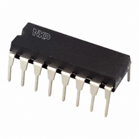
... NXP Semiconductors DIP16: plastic dual in-line package; 16 leads (300 mil pin 1 index 1 DIMENSIONS (inch dimensions are derived from the original mm dimensions UNIT max. min. max. mm 4.2 0.51 3.2 inches 0.17 0.02 0.13 Note 1. Plastic or metal protrusions of 0.25 mm (0.01 inch) maximum per side are not included. ...
Page 26
... NXP Semiconductors TSSOP16: plastic thin shrink small outline package; 16 leads; body width 4 pin 1 index 1 DIMENSIONS (mm are the original dimensions) A UNIT max. 0.15 0.95 mm 1.1 0.25 0.05 0.80 Notes 1. Plastic or metal protrusions of 0.15 mm maximum per side are not included. 2. Plastic interlead protrusions of 0.25 mm maximum per side are not included. ...
Page 27
... Release date 74HC_HCT193_3 20070523 • Modifications: The format of this data sheet has been redesigned to comply with the new identity guidelines of NXP Semiconductors. • Legal texts have been adapted to the new company name where appropriate. • Family specification included 74HC_HCT193_CNV_2 ...
Page 28
... For detailed and full information see the relevant full data sheet, which is available on request via the local NXP Semiconductors sales office. In case of any inconsistency or conflict with the short data sheet, the full data sheet shall prevail ...
Page 29
... NXP Semiconductors 18. Contents 1 General description . . . . . . . . . . . . . . . . . . . . . . 1 2 Features . . . . . . . . . . . . . . . . . . . . . . . . . . . . . . . 2 3 Ordering information . . . . . . . . . . . . . . . . . . . . . 2 4 Functional diagram . . . . . . . . . . . . . . . . . . . . . . 2 5 Pinning information . . . . . . . . . . . . . . . . . . . . . . 5 5.1 Pinning . . . . . . . . . . . . . . . . . . . . . . . . . . . . . . . 5 5.2 Pin description . . . . . . . . . . . . . . . . . . . . . . . . . 5 6 Functional description . . . . . . . . . . . . . . . . . . . 6 7 Limiting values Recommended operating conditions Static characteristics Dynamic characteristics . . . . . . . . . . . . . . . . . 13 11 Waveforms . . . . . . . . . . . . . . . . . . . . . . . . . . . . 18 12 Application information Package outline . . . . . . . . . . . . . . . . . . . . . . . . 23 14 Revision history ...