M74HC590B1R STMicroelectronics, M74HC590B1R Datasheet
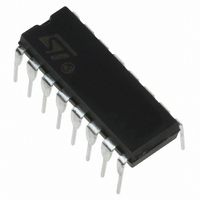
IC COUNTER REGISTER 8BIN 16-DIP

M74HC590B1R

Manufacturer Part Number
M74HC590B1R
Description
IC COUNTER REGISTER 8BIN 16-DIP
Manufacturer
STMicroelectronics
Series
74HCr
Datasheets

Specifications of M74HC590B1R

Logic Type
Binary Counter
Direction
Up
Number Of Elements
1
Number Of Bits Per Element
8
Reset
Asynchronous
Count Rate
61MHz
Trigger Type
Positive Edge
Voltage - Supply
2 V ~ 6 V
Operating Temperature
-55°C ~ 125°C
Mounting Type
Through Hole
Package / Case
16-DIP (0.300", 7.62mm)
Counter Type
Binary
Counting Sequence
Up
Number Of Circuits
8
Logic Family
74HC
Output Type
3-State
Propagation Delay Time
185 ns, 37 ns, 31 ns
Supply Voltage (max)
6 V
Maximum Operating Temperature
+ 125 C
Minimum Operating Temperature
- 55 C
Function
Register
Mounting Style
Through Hole
Operating Supply Voltage
2 V to 6 V
Circuit Type
Silicon Gate
Current, Supply
80 μA
Function Type
8-Bits
Logic Function
Counter/Register
Package Type
DIP-16
Special Features
Binary, High Speed, Parallel, Tri-State
Temperature, Operating, Range
-55 to +125 °C
Voltage, Supply
2 to 6 V
Lead Free Status / RoHS Status
Lead free / RoHS Compliant
Timing
-
Lead Free Status / Rohs Status
Lead free / RoHS Compliant
Other names
497-1879-5

Available stocks

Company
Part Number
Manufacturer
Quantity
Price
Part Number:
M74HC590B1R
Manufacturer:
GSI
Quantity:
132
DESCRIPTION
The M74HC590 is an high speed CMOS 8-BIT
BINARY COUNTER REGISTER (3 STATE)
fabricated with silicon gate C
This device contains an 8-bit binary counter that
feeds an 8-bit storage register. The storage
register has parallel outputs. Separate clocks are
provided for both the binary counter and storage
register. The binary counter features a direct clear
input CCLR and a count enable input CCKEN. For
PIN CONNECTION AND IEC LOGIC SYMBOLS
August 2001
HIGH SPEED:
f
LOW POWER DISSIPATION:
I
HIGH NOISE IMMUNITY:
V
SYMMETRICAL OUTPUT IMPEDANCE:
|I
|I
BALANCED PROPAGATION DELAYS:
t
WIDE OPERATING VOLTAGE RANGE:
V
PIN AND FUNCTION COMPATIBLE WITH
74 SERIES 590
MAX
CC
PLH
OH
OH
NIH
CC
= 4 A(MAX.) at T
| = I
| = I
(OPR) = 2V to 6V
= 61 MHz (TYP.) at V
= V
t
PHL
OL
OL
NIL
= 6mA (MIN) for QA ~ QH OUTPUT
= 4mA (MIN) for RCO OUTPUT
= 28 % V
A
CC
=25°C
(MIN.)
2
CC
MOS technology.
= 6V
8 BINARY COUNTER REGISTER
ORDER CODES
cascading, a ripple carry output RCO is provided.
Expansion is easily accomplished by tying RCO of
the first stage to CCKEN of the second stage, etc.
Both the counter and register clocks are positive
edge triggered. If the user wishes to connect both
clocks together, the counter state will always be
one count ahead of the register. Internal circuitry
prevents clocking from the clock enable. All inputs
are equipped with protection circuits against static
discharge and transient excess voltage.
PACKAGE
TSSOP
SOP
DIP
WITH 3 STATE OUTPUT
DIP
M74HC590M1R
M74HC590B1R
TUBE
SOP
M74HC590
M74HC590RM13TR
M74HC590TTR
T & R
TSSOP
1/15

Related parts for M74HC590B1R

M74HC590B1R Summary of contents

Page 1

... Internal circuitry prevents clocking from the clock enable. All inputs are equipped with protection circuits against static discharge and transient excess voltage. M74HC590 WITH 3 STATE OUTPUT DIP SOP TUBE T & R M74HC590B1R M74HC590M1R M74HC590RM13TR M74HC590TTR TSSOP 1/15 ...

Page 2

M74HC590 INPUT AND OUTPUT EQUIVALENT CIRCUIT TRUTH TABLE INPUTS G RCK CCLR Don’t Care RCO = QA’·QB’·QC’·QD’·QE’·QF’·QG’·QH’ ...

Page 3

LOGIC DIAGRAM This logic diagram has not be used to estimate propagation delays M74HC590 3/15 ...

Page 4

M74HC590 TIMING CHART 4/15 ...

Page 5

ABSOLUTE MAXIMUM RATINGS Symbol V Supply Voltage Input Voltage Output Voltage Input Diode Current Output Diode Current OK DC Output Source Sink Current per Output PIN (RCO) I ...

Page 6

M74HC590 DC SPECIFICATIONS Symbol Parameter V V High Level Input IH Voltage V Low Level Input IL Voltage V High Level Output OH Voltage (for RCO Output) V High Level Output OH Voltage (for Outputs) V Low ...

Page 7

AC ELECTRICAL CHARACTERISTICS (C Symbol Parameter Output Transition TLH THL Time t t Output Transition TLH THL Time (RCO Propagation Delay PLH PHL Time (CCK - RCO) t Propagation Delay PLH Time (CCLR - RCO) ...

Page 8

M74HC590 Symbol Parameter V t Minimum Removal REM Time (CCLR) CAPACITIVE CHARACTERISTICS Symbol Parameter V C Input Capacitance IN C Power Dissipation PD Capacitance (note defined as the value of the IC’s internal equivalent capacitance which ...

Page 9

WAVEFORM 1 : PROPAGATION DELAY, MINIMUM PULSE WIDTH (f=1MHz; 50% duty cycle) WAVEFORM 2 : MINIMUM SETUP AND HOLD TIME (f=1MHz; 50% duty cycle) M74HC590 9/15 ...

Page 10

M74HC590 WAVEFORM 3 : PROPAGATION DELAY TIME (f=1MHz; 50% duty cycle) WAVEFORM 4 : MINIMUM SETUP AND HOLD TIME (f=1MHz; 50% duty cycle) 10/15 ...

Page 11

WAVEFORM 5 : MINIMUM PULSE WIDTH, REMOVAL TIME (f=1MHz; 50% duty cycle) WAVEFORM 6 : OUTPUT ENABLE AND DISABLE TIME (f=1MHz; 50% duty cycle) M74HC590 11/15 ...

Page 12

M74HC590 DIM. MIN. a1 0. 12/15 Plastic DIP-16 (0.25) MECHANICAL DATA mm. TYP MAX. 1.65 0.5 0.25 20 8.5 2.54 17.78 7.1 5.1 3.3 1.27 inch MIN. TYP. ...

Page 13

SO-16 MECHANICAL DATA mm. DIM. MIN 0 0. 9 3.8 G 4 TYP MAX. MIN. 1.75 0.2 0.003 1.65 0.46 0.013 0.25 ...

Page 14

M74HC590 DIM. MIN 0.05 A2 0.8 b 0.19 c 0.09 D 4.9 E 6 0° PIN 1 IDENTIFICATION 1 14/15 TSSOP16 MECHANICAL DATA mm. TYP MAX. 1.2 0.15 ...

Page 15

... No license is granted by implication or otherwise under any patent or patent rights of STMicroelectronics. Specifications mentioned in this publication are subject to change without notice. This publication supersedes and replaces all information previously supplied ...

Related keywords