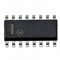
MC74HC4020ADG ON Semiconductor, MC74HC4020ADG Datasheet

MC74HC4020ADG
Specifications of MC74HC4020ADG
Available stocks
Related parts for MC74HC4020ADG
MC74HC4020ADG Summary of contents
Page 1
MC74HC4020A 14-Stage Binary Ripple Counter High−Performance Silicon−Gate CMOS The MC74C4020A is identical in pinout to the standard CMOS MC14020B. The device inputs are compatible with standard CMOS outputs; with pullup resistors, they are compatible with LSTTL outputs. This device consists ...
Page 2
... Pin Reset Pin 8 = GND Figure 1. Logic Diagram ORDERING INFORMATION Device MC74HC4020AN MC74HC4020ANG MC74HC4020AD MC74HC4020ADG MC74HC4020ADR2 MC74HC4020ADR2G MC74HC4020ADTR2 MC74HC4020ADTR2G MC74HC4020AF MC74HC4020AFG MC74HC4020AFEL MC74HC4020AFELG †For information on tape and reel specifications, including part orientation and tape sizes, please refer to our Tape and Reel Packaging Specifications Brochure, BRD8011/D. *This package is inherently Pb− ...
Page 3
... Plastic DIP: – 10 mW/_C from 65_ to 125_C SOIC Package: – 7 mW/_C from 65_ to 125_C TSSOP Package: − 6.1 mW/_C from 65_ to 125_C For high frequency or heavy load considerations, see Chapter 2 of the ON Semiconductor High−Speed CMOS Data Book (DL129/D). RECOMMENDED OPERATING CONDITIONS Î Î Î Î ...
Page 4
DC CHARACTERISTICS (Voltages Referenced to GND) Symbol Parameter V Minimum High−Level Input Voltage IH V Maximum Low−Level Input Voltage IL V Minimum High−Level Output Voltage OH V Maximum Low−Level Output Voltage OL I Maximum Input Leakage Current in I Maximum ...
Page 5
AC CHARACTERISTICS ( pF, Input t L Symbol f Maximum Clock Frequency (50% Duty Cycle) max (Figures 1 and Maximum Propagation Delay, Clock to Q1* PLH t (Figures 1 and 4) PHL t Maximum Propagation ...
Page 6
... Maximum Input Rise and Fall Times r f (Figure 1) NOTE: Information on typical parametric values can be found in Chapter 2 of the ON Semiconductor High−Speed CMOS Data Book (DL129/D). INPUTS Clock (Pin 10) Negative−edge triggering clock input. A high−to−low transition on this input advances the state of the counter. ...
Page 7
Qn 50% t PLH Qn+1 50% Figure Clock Reset Q6 = Pin Pin Pin 13 SWITCHING WAVEFORMS (continued GND t PHL Q4 Q5 ...
Page 8
Clock Reset Q10 Q12 Q13 Q14 Time−Base Generator A 60Hz sinewave obtained through a 1.0 Megohm resistor connected directly to a standard 120 Vac power line is applied to the ...
Page 9
−T− 0.25 (0.010 PACKAGE DIMENSIONS PDIP−16 N SUFFIX CASE 648−08 ISSUE T L SEATING PLANE http://onsemi.com 9 NOTES: 1. ...
Page 10
... G K −T− SEATING PLANE 0.25 (0.010 *For additional information on our Pb−Free strategy and soldering details, please download the ON Semiconductor Soldering and Mounting Techniques Reference Manual, SOLDERRM/D. PACKAGE DIMENSIONS SOIC−16 CASE 751B−05 ISSUE K −B− 0.25 (0.010 SOLDERING FOOTPRINT 8X 6 ...
Page 11
... −V− C 0.10 (0.004) −T− SEATING D PLANE 16X 0.36 *For additional information on our Pb−Free strategy and soldering details, please download the ON Semiconductor Soldering and Mounting Techniques Reference Manual, SOLDERRM/D. PACKAGE DIMENSIONS TSSOP−16 CASE 948F−01 ISSUE É É É ...
Page 12
... Opportunity/Affirmative Action Employer. This literature is subject to all applicable copyright laws and is not for resale in any manner. PUBLICATION ORDERING INFORMATION LITERATURE FULFILLMENT: Literature Distribution Center for ON Semiconductor P.O. Box 5163, Denver, Colorado 80217 USA Phone: 303−675−2175 or 800−344−3860 Toll Free USA/Canada Fax: 303− ...


