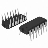
MC74HC393ANG ON Semiconductor, MC74HC393ANG Datasheet

MC74HC393ANG
Specifications of MC74HC393ANG
Related parts for MC74HC393ANG
MC74HC393ANG Summary of contents
Page 1
MC74HC393A Dual 4−Stage Binary Ripple Counter High−Performance Silicon−Gate CMOS The MC74HC393A is identical in pinout to the LS393. The device inputs are compatible with standard CMOS outputs; with pullup resistors, they are compatible with LSTTL outputs. This device consists of ...
Page 2
... GND ORDERING INFORMATION Device MC74HC393AN MC74HC393ANG MC74HC393AD MC74HC393ADG MC74HC393ADR2 MC74HC393ADR2G MC74HC393ADTR2 MC74HC393ADTR2G MC74HC393AFEL MC74HC393AFELG †For information on tape and reel specifications, including part orientation and tape sizes, please refer to our Tape and Reel Packaging Specifications Brochure, BRD8011/D. *This package is inherently Pb−Free CLOCK ...
Page 3
... Plastic DIP: – 10 mW/_C from 65_ to 125_C SOIC Package: – 7 mW/_C from 65_ to 125_C TSSOP Package: − 6.1 mW/_C from 65_ to 125_C For high frequency or heavy load considerations, see Chapter 2 of the ON Semiconductor High−Speed CMOS Data Book (DL129/D). RECOMMENDED OPERATING CONDITIONS Î Î Î Î ...
Page 4
... NOTES: 1. For propagation delays with loads other than 50 pF, see Chapter 2 of the ON Semiconductor High−Speed CMOS Data Book (DL129/D). 2. Information on typical parametric values can be found in Chapter 2 of the ON Semiconductor High−Speed CMOS Data Book (DL129/D). ...
Page 5
... NOTE: Information on typical parametric values can be found in Chapter 2 of the ON Semiconductor High−Speed CMOS Data Book (DL129/D). INPUTS Clock (Pins 1, 13) Clock input. The internal flip− ...
Page 6
CLOCK 10 1/f max t t PLH PHL 90% Q 50% 10 TLH THL Figure 1. TEST POINT OUTPUT DEVICE UNDER C TEST *Includes all probe and jig capacitance ...
Page 7
CLOCK RESET Count TIMING DIAGRAM COUNT SEQUENCE Outputs Q4 ...
Page 8
−T− SEATING PLANE 0.13 (0.005) PACKAGE DIMENSIONS PDIP−14 CASE 646−06 ISSUE http://onsemi.com 8 NOTES: 1. DIMENSIONING AND TOLERANCING PER ANSI ...
Page 9
... G −T− SEATING 14 PL PLANE 0.25 (0.010 14X 0.58 *For additional information on our Pb−Free strategy and soldering details, please download the ON Semiconductor Soldering and Mounting Techniques Reference Manual, SOLDERRM/D. PACKAGE DIMENSIONS SOIC−14 CASE 751A−03 ISSUE 0.25 (0.010 ...
Page 10
... S A −V− C 0.10 (0.004) −T− SEATING G D PLANE 14X 0.36 *For additional information on our Pb−Free strategy and soldering details, please download the ON Semiconductor Soldering and Mounting Techniques Reference Manual, SOLDERRM/D. PACKAGE DIMENSIONS TSSOP−14 CASE 948G−01 ISSUE 0.25 (0.010) ...
Page 11
... Opportunity/Affirmative Action Employer. This literature is subject to all applicable copyright laws and is not for resale in any manner. PUBLICATION ORDERING INFORMATION LITERATURE FULFILLMENT: Literature Distribution Center for ON Semiconductor P.O. Box 5163, Denver, Colorado 80217 USA Phone: 303−675−2175 or 800−344−3860 Toll Free USA/Canada Fax: 303− ...


