HCF4510BEY STMicroelectronics, HCF4510BEY Datasheet
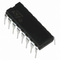
IC COUNTER PRESET UP/DOWN 16-DIP

HCF4510BEY

Manufacturer Part Number
HCF4510BEY
Description
IC COUNTER PRESET UP/DOWN 16-DIP
Manufacturer
STMicroelectronics
Series
4000Br
Datasheet

Specifications of HCF4510BEY

Logic Type
BCD Counter
Direction
Up, Down
Number Of Elements
1
Number Of Bits Per Element
4
Reset
Asynchronous
Timing
Synchronous
Count Rate
11MHz
Trigger Type
Positive Edge
Voltage - Supply
3 V ~ 20 V
Operating Temperature
-55°C ~ 125°C
Mounting Type
Through Hole
Package / Case
16-DIP (0.300", 7.62mm)
Lead Free Status / RoHS Status
Lead free / RoHS Compliant

Available stocks

Company
Part Number
Manufacturer
Quantity
Price
Part Number:
HCF4510BEY
Manufacturer:
NXP
Quantity:
340
Part Number:
HCF4510BEY
Manufacturer:
ST
0
DESCRIPTION
HCF4510B is a monolithic integrated circuit
fabricated
technology available in DIP package.
It
COUNTER
clocked D-type flip-flops (with a gating structure to
provide T-type flip-flop capability) connected as a
counter. This counter can be cleared by a high
level on the RESET line, and can be preset to any
binary number present on the jam inputs by a high
level on the PRESET ENABLE line. This device
will count out of non-BCD counter states in a
maximum of two clock pulses in the up mode and
PIN CONNECTION
September 2002
MEDIUM SPEED OPERATION :
8 MHz (Typ.) at 10V
SYNCHRONOUS INTERNAL CARRY
PROPAGATION
RESET AND PRESET CAPABILITY
STANDARDIZED SYMMETRICAL OUTPUT
CHARACTERISTICS
QUIESCENT CURRENT SPECIF. UP TO 20V
5V, 10V AND 15V PARAMETRIC RATINGS
INPUT LEAKAGE CURRENT
I
100% TESTED FOR QUIESCENT CURRENT
MEETS ALL REQUIREMENTS OF JEDEC
JESD13B "STANDARD SPECIFICATIONS
FOR DESCRIPTION OF B SERIES CMOS
DEVICES"
I
is
= 100nA (MAX) AT V
a
PRESETTABLE
in
consists
Metal
of
Oxide
DD
four
= 18V T
PRESETTABLE BCD UP/DOWN COUNTER
BCD
Semiconductor
synchronously
A
UP/DOWN
= 25°C
ORDER CODES
a maximum of four clock pulses in the down mode.
If the CARRY IN input is held low, the counter
advances up or down on each positive going clock
transition.
accomplished by connecting all clock inputs in
parallel and connecting the CARRY OUT of a less
significant stage to the CARRY IN of a more
significant stage. HCF4510B can be cascaded in
the ripple mode by connecting all clock inputs in
parallel and connecting the CARRY OUT to the
clock of the next stage. If the UP/DOWN input
changes during a terminal count, the CARRY OUT
must be gated with the clock, and the UP/DOWN
input must change while the clock is high. This
method provides a clean clock signal to the
subsequent counting stage.
PACKAGE
DIP
HCF4510BEY
Synchronous
TUBE
DIP
HCF4510B
cascading
T & R
1/11
is

Related parts for HCF4510BEY

HCF4510BEY Summary of contents

Page 1

... If the UP/DOWN input changes during a terminal count, the CARRY OUT must be gated with the clock, and the UP/DOWN input must change while the clock is high. This method provides a clean clock signal to the subsequent counting stage. HCF4510B DIP TUBE T & R HCF4510BEY Synchronous cascading is 1/11 ...

Page 2

HCF4510B IINPUT EQUIVALENT CIRCUIT FUNCTIONAL DIAGRAM TRUTH TABLE CARRY-IN CL (Cl Don’t Care 2/11 PIN DESCRIPTION PIN 12, 13 11, 14 ...

Page 3

LOGIC DIAGRAM TIMING CHART HCF4510B 3/11 ...

Page 4

HCF4510B ABSOLUTE MAXIMUM RATINGS Symbol V Supply Voltage Input Voltage Input Current I P Power Dissipation per Package D Power Dissipation per Output Transistor T Operating Temperature op T Storage Temperature stg Absolute Maximum ...

Page 5

DC SPECIFICATIONS Symbol Parameter V (V) I Quiescent Current 0/5 L 0/10 0/15 0/20 V High Level Output 0/5 OH Voltage 0/10 0/15 V Low Level Output 5/0 OL Voltage 10/0 15/0 V High Level Input IH Voltage V Low ...

Page 6

HCF4510B DYNAMIC ELECTRICAL CHARACTERISTICS (T Symbol Parameter t t Propagation Delay Time PHL PLH Clock to Q Output t t Propagation Delay Time PHL PLH Preset or Reset to Q Output t t Propagation Delay Time PHL PLH Clock to ...

Page 7

TEST CIRCUIT C = 50pF or equivalent (includes jig and probe capacitance 200K pulse generator (typically OUT WAVEFORM 1 : PROPAGATION DELAY TIMES (f=1MHz; 50% duty cycle) HCF4510B 7/11 ...

Page 8

HCF4510B WAVEFORM 2 : MINIMUM SETUP TIME (CI TO CLOCK) (f=1MHz; 50% duty cycle) WAVEFORM 3 : PROPAGATION DELAY TIMES, MINIMUM RESET PULSE WIDTH (f=1MHz; 50% duty cycle) 8/11 ...

Page 9

TIPICAL APPLICATIONS TYPICAL 16-CHANNEL, 10 BIT DATA ACQUISITION SYSTEM TIPICAL APPLICATIONS CASCADING COUNTER PACKAGES HCF4510B 9/11 ...

Page 10

HCF4510B DIM. MIN. a1 0. 10/11 Plastic DIP-16 (0.25) MECHANICAL DATA mm. TYP MAX. 1.65 0.5 0.25 20 8.5 2.54 17.78 7.1 5.1 3.3 1.27 inch MIN. TYP. ...

Page 11

... No license is granted by implication or otherwise under any patent or patent rights of STMicroelectronics. Specifications mentioned in this publication are subject to change without notice. This publication supersedes and replaces all information previously supplied ...

Related keywords