CD4013BCN Fairchild Semiconductor, CD4013BCN Datasheet

IC FLIP FLOP DUAL D 14-DIP

CD4013BCN

Manufacturer Part Number
CD4013BCN
Description
IC FLIP FLOP DUAL D 14-DIP
Manufacturer
Fairchild Semiconductor
Series
4000Br
Type
D-Typer
Datasheets

Specifications of CD4013BCN

Function
Set(Preset) and Reset
Output Type
Differential
Number Of Elements
2
Number Of Bits Per Element
1
Frequency - Clock
12.5MHz
Delay Time - Propagation
65ns
Trigger Type
Positive Edge
Current - Output High, Low
8.8mA, 8.8mA
Voltage - Supply
3 V ~ 15 V
Operating Temperature
-55°C ~ 125°C
Mounting Type
Through Hole
Package / Case
14-DIP (0.300", 7.62mm)
Number Of Circuits
2
Logic Family
CD401
Logic Type
D-Type Flip-Flop
Polarity
Inverting/Non-Inverting
Input Type
Single-Ended
Propagation Delay Time
350 ns
High Level Output Current
- 4.2 mA
Low Level Output Current
4.2 mA
Supply Voltage (max)
15 V
Maximum Operating Temperature
+ 85 C
Mounting Style
Through Hole
Minimum Operating Temperature
- 40 C
Supply Voltage (min)
3 V
Technology
CMOS
Number Of Bits
2
Number Of Elements
2
Clock-edge Trigger Type
Positive-Edge
Operating Supply Voltage (typ)
3.3/5/9/12V
Package Type
PDIP
Frequency (max)
15.5MHz
Operating Supply Voltage (min)
3V
Operating Supply Voltage (max)
15V
Operating Temp Range
-55C to 125C
Operating Temperature Classification
Military
Mounting
Through Hole
Pin Count
14
Lead Free Status / RoHS Status
Lead free / RoHS Compliant
Other names
4013
4013
4013B
CD4013
MM5613BCN

Available stocks

Company
Part Number
Manufacturer
Quantity
Price
Part Number:
CD4013BCN
Manufacturer:
TI/德州仪器
Quantity:
20 000
© 1999 Fairchild Semiconductor Corporation
CD4013BCM
CD4013BCSJ
CD4013BCN
CD4013BC
Dual D-Type Flip-Flop
General Description
The CD4013B dual D-type flip-flop is a monolithic comple-
mentary MOS (CMOS) integrated circuit constructed with
N- and P-channel enhancement mode transistors. Each
flip-flop has independent data, set, reset, and clock inputs
and “Q” and “Q” outputs. These devices can be used for
shift register applications, and by connecting “Q” output to
the data input, for counter and toggle applications. The
logic level present at the “D” input is transferred to the Q
output during the positive-going transition of the clock
pulse. Setting or resetting is independent of the clock and
is accomplished by a high level on the set or reset line
respectively.
Ordering Code:
Devices also available in Tape and Reel. Specify by appending the suffix letter “X” to the ordering code.
Connection Diagram
Order Number
Pin Assignments for DIP, SOIC and SOP
Package Number
Top View
M14A
M14D
N14A
14-Lead Small Outline Integrated Circuit (SOIC), JEDEC MS-120, 0.150” Narrow
14-Lead Small Outline Package (SOP), EIAJ TYPE II, 5.3mm Wide
14-Lead Dual-In-Line Package (PDIP), JEDEC MS-001, 0.300” Wide
DS005946.prf
Features
Applications
• Automotive
• Data terminals
• Instrumentation
• Medical electronics
• Alarm system
• Industrial electronics
• Remote metering
• Computers
Truth Table
No Change
x
Note 1: Level Change
Wide supply voltage range:
High noise immunity: 0.45 V
Low power TTL: fan out of 2 driving 74L
Don't Care Case
(Note 1)
compatibility: or 1 driving 74LS
CL


x
x
x
Package Description
D
0
1
x
x
x
x
R
0
0
0
1
0
1
October 1987
Revised January 1999
DD
3.0V to 15V
S
0
0
0
0
1
1
(typ.)
www.fairchildsemi.com
Q
Q
0
1
0
1
1
Q
Q
1
0
1
0
1

Related parts for CD4013BCN

CD4013BCN Summary of contents

Page 1

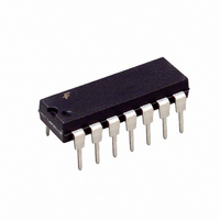
... Small Outline Integrated Circuit (SOIC), JEDEC MS-120, 0.150” Narrow CD4013BCSJ M14D 14-Lead Small Outline Package (SOP), EIAJ TYPE II, 5.3mm Wide CD4013BCN N14A 14-Lead Dual-In-Line Package (PDIP), JEDEC MS-001, 0.300” Wide Devices also available in Tape and Reel. Specify by appending the suffix letter “X” to the ordering code. ...

Page 2

Schematic Diagrams www.fairchildsemi.com Logic Diagram 2 ...

Page 3

Absolute Maximum Ratings (Note 3) DC Supply Voltage ( Input Voltage ( Storage Temperature Range ( Power Dissipation ( Dual-In-Line Small Outline ) Lead Temperature (T L ...

Page 4

AC Electrical Characteristics pF, R 200k, unless otherwise noted Symbol Parameter CLOCK OPERATION Propagation Delay Time PHL PLH Transition Time THL TLH Minimum ...

Page 5

Physical Dimensions inches (millimeters) unless otherwise noted 14-Lead Small Outline Integrated Circuit (SOIC), JEDEC MS-120, 0.150” Narrow 14-Lead Small Outline Package (SOP), EIAJ TYPE II, 5.3mm Wide Package Number M14A Package Number M14D 5 www.fairchildsemi.com ...

Page 6

Physical Dimensions inches (millimeters) unless otherwise noted (Continued) 14-Lead Plastic Dual-In-Line Package (PDIP), JEDEC MS-001, 0.300” Wide LIFE SUPPORT POLICY FAIRCHILD’S PRODUCTS ARE NOT AUTHORIZED FOR USE AS CRITICAL COMPONENTS IN LIFE SUPPORT DEVICES OR SYSTEMS WITHOUT THE EXPRESS WRITTEN ...

Related keywords