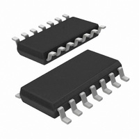
HEF4013BT,653 NXP Semiconductors, HEF4013BT,653 Datasheet - Page 3

HEF4013BT,653
Manufacturer Part Number
HEF4013BT,653
Description
IC FLIP FLOP DUAL DTYPE 14SOIC
Manufacturer
NXP Semiconductors
Series
4000Br
Type
D-Typer
Specifications of HEF4013BT,653
Package / Case
14-SOIC (3.9mm Width), 14-SOL
Function
Set(Preset) and Reset
Output Type
Differential
Number Of Elements
2
Number Of Bits Per Element
1
Frequency - Clock
40MHz
Trigger Type
Positive Edge
Current - Output High, Low
3.4mA, 3.4mA
Voltage - Supply
3 V ~ 15 V
Operating Temperature
-40°C ~ 125°C
Mounting Type
Surface Mount
Number Of Circuits
2
Logic Family
HEF4000
Logic Type
D-Type Edge Triggered Flip-Flop
Polarity
Inverting/Non-Inverting
Input Type
Single-Ended
Propagation Delay Time
30 ns at 15 V
High Level Output Current
- 4.2 mA
Low Level Output Current
4.2 mA
Supply Voltage (max)
15.5 V
Maximum Operating Temperature
+ 125 C
Mounting Style
SMD/SMT
Minimum Operating Temperature
- 40 C
Supply Voltage (min)
4.5 V
Lead Free Status / RoHS Status
Lead free / RoHS Compliant
Delay Time - Propagation
-
Lead Free Status / Rohs Status
Lead free / RoHS Compliant
Other names
933372660653
HEF4013BTD-T
HEF4013BTD-T
HEF4013BTD-T
HEF4013BTD-T
Available stocks
Company
Part Number
Manufacturer
Quantity
Price
Part Number:
HEF4013BT,653
Manufacturer:
NEXPERIA/安世
Quantity:
20 000
NXP Semiconductors
6. Pinning information
Table 2.
7. Functional description
Table 3.
[1]
HEF4013B_6
Product data sheet
Symbol
1Q, 2Q
1Q, 2Q
1CP, 2CP
1CD, 2CD
1D, 2D
1SD, 2SD
V
V
Control
nSD
H
L
H
L
L
Fig 3.
SS
DD
H = HIGH voltage level; L = LOW voltage level; X = don’t care;
Pin configuration
Pin description
Function table
6.1 Pinning
6.2 Pin description
nCD
L
H
H
L
L
Pin
1, 13
2, 12
3, 11
4, 10
5, 9
6, 8
7
14
[1]
nCP
X
X
X
Description
true output
complement output
clock input (LOW to HIGH edge-triggered)
asynchronous clear-direct input (active HIGH)
data input
asynchronous set-direct input (active HIGH)
ground (0 V)
supply voltage
1CD
1CP
1SD
V
1Q
1Q
1D
SS
Rev. 06 — 27 October 2009
1
2
3
4
5
6
7
HEF4013B
= LOW-to-HIGH clock transition.
001aag085
Input
nD
X
X
X
L
H
14
13
12
11
10
9
8
V
2Q
2Q
2CP
2CD
2D
2SD
DD
Output
nQ
H
L
H
L
H
HEF4013B
Dual D-type flip-flop
© NXP B.V. 2009. All rights reserved.
nQ
L
H
H
H
L
3 of 15


