MC14076BCPG ON Semiconductor, MC14076BCPG Datasheet
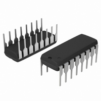
IC FLIP FLOP QUAD TYPE D 16-DIP

MC14076BCPG

Manufacturer Part Number
MC14076BCPG
Description
IC FLIP FLOP QUAD TYPE D 16-DIP
Manufacturer
ON Semiconductor
Series
4000Br
Type
D-Type Busr
Datasheet

Specifications of MC14076BCPG

Function
Master Reset
Output Type
Non-Inverted
Number Of Elements
1
Number Of Bits Per Element
4
Frequency - Clock
12MHz
Trigger Type
Positive Edge
Current - Output High, Low
8.8mA, 8.8mA
Voltage - Supply
3 V ~ 18 V
Operating Temperature
-55°C ~ 125°C
Mounting Type
Through Hole
Package / Case
16-DIP (0.300", 7.62mm)
Logic Family
4000
Technology
CMOS
Number Of Bits
4
Number Of Elements
1
Clock-edge Trigger Type
Positive-Edge
Polarity
Non-Inverting
Operating Supply Voltage (typ)
3.3/5/9/12/15V
Package Type
PDIP
Propagation Delay Time
600ns
Low Level Output Current
4.2mA
High Level Output Current
-4.2mA
Frequency (max)
6MHz
Operating Supply Voltage (min)
3V
Operating Supply Voltage (max)
18V
Operating Temp Range
-55C to 125C
Operating Temperature Classification
Military
Mounting
Through Hole
Pin Count
16
Lead Free Status / RoHS Status
Lead free / RoHS Compliant
Delay Time - Propagation
-
Lead Free Status / Rohs Status
Compliant
Other names
MC14076BCPG
MC14076BCPGOS
MC14076B
4-Bit D-Type Register
with Three-State Outputs
operating synchronously from a common clock. OR gated
output−disable inputs force the outputs into a high−impedance state
for use in bus organized systems. OR gated data−disable inputs cause
the Q outputs to be fed back to the D inputs of the flip−flops. Thus they
are inhibited from changing state while the clocking process remains
undisturbed. An asynchronous master root is provided to clear all four
flip−flops simultaneously independent of the clock or disable inputs.
Features
Stresses exceeding Maximum Ratings may damage the device. Maximum
Ratings are stress ratings only. Functional operation above the Recommended
Operating Conditions is not implied. Extended exposure to stresses above the
Recommended Operating Conditions may affect device reliability.
1. Temperature Derating:
static voltages or electric fields. However, precautions must be taken to avoid
applications of any voltage higher than maximum rated voltages to this
high−impedance circuit. For proper operation, V
to the range V
(e.g., either V
*For additional information on our Pb−Free strategy and soldering details, please
MAXIMUM RATINGS
© Semiconductor Components Industries, LLC, 2009
September, 2009 − Rev. 6
Symbol
V
download the ON Semiconductor Soldering and Mounting Techniques
Reference Manual, SOLDERRM/D.
I
The MC14076B 4−Bit Register consists of four D−type flip−flops
in
in
This device contains protection circuitry to guard against damage due to high
Unused inputs must always be tied to an appropriate logic voltage level
Modes: Parallel Load and Do Nothing
Schottky TTL Load Over the Rated Temperature Range
Three−State Outputs with Gated Control Lines
Fully Independent Clock Allows Unrestricted Operation for the Two
Asynchronous Master Reset
Four Bus Buffer Registers
Supply Voltage Range = 3.0 Vdc to 18 Vdc
Capable of Driving Two Low−Power TTL Loads or One Low−Power
These are Pb−Free Devices*
V
T
Plastic “P and D/DW” Packages: – 7.0 mW/_C From 65_C To 125_C
P
, V
, I
T
T
DD
stg
D
A
L
out
out
DC Supply Voltage Range
Input or Output Voltage Range
Input or Output Current
Power Dissipation, per Package
Ambient Temperature Range
Storage Temperature Range
Lead Temperature
SS
SS
(DC or Transient)
(DC or Transient) per Pin
(Note 1)
(8−Second Soldering)
or V
v (V
DD
in
). Unused outputs must be left open.
Parameter
or V
(Voltages Referenced to V
out
) v V
DD
.
in
and V
−0.5 to V
SS
−0.5 to +18.0
−55 to +125
−65 to +150
out
)
Value
± 10
should be constrained
500
260
DD
+ 0.5
1
Unit
mW
mA
°C
°C
°C
V
V
See detailed ordering and shipping information in the package
dimensions section on page 3 of this data sheet.
ORDERING INFORMATION
A
WL, L
YY, Y
WW, W
G
http://onsemi.com
CASE 751B
CASE 648
P SUFFIX
D SUFFIX
PDIP−16
SOIC−16
= Assembly Location
= Wafer Lot
= Year
= Work Week
= Pb−Free Package
Publication Order Number:
16
1
16
1
DIAGRAMS
MARKING
MC14076BCP
AWLYYWWG
AWLYWW
MC14076B/D
14076BG

Related parts for MC14076BCPG

MC14076BCPG Summary of contents

Page 1

... Unused inputs must always be tied to an appropriate logic voltage level (e.g., either Unused outputs must be left open *For additional information on our Pb−Free strategy and soldering details, please download the ON Semiconductor Soldering and Mounting Techniques Reference Manual, SOLDERRM/D. © Semiconductor Components Industries, LLC, 2009 September, 2009 − Rev Value Unit − ...

Page 2

PIN ASSIGNMENT { OUTPUT DISABLE ...

Page 3

... ORDERING INFORMATION Device MC14076BCPG MC14076BDG MC14076BDR2G †For information on tape and reel specifications, including part orientation and tape sizes, please refer to our Tape and Reel Packaging Specifications Brochure, BRD8011/D. Package PDIP−16 (Pb−Free) SOIC−16 (Pb−Free) SOIC−16 (Pb−Free) http://onsemi.com 3 † ...

Page 4

ELECTRICAL CHARACTERISTICS Î Î Î Î Î ...

Page 5

SWITCHING CHARACTERISTICS (Note 5) Î Î Î ...

Page 6

INPUT RISE AND FALL 20 ns 90% INPUT D 50% INFORMATION 10 50 PLH 90% Q OUTPUT 10% t TLH RESET = 0 DATA DISABLE A AND ...

Page 7

−T− 0.25 (0.010 PACKAGE DIMENSIONS PDIP−16 P SUFFIX CASE 648−08 ISSUE T L SEATING PLANE http://onsemi.com 7 NOTES: 1. ...

Page 8

... Opportunity/Affirmative Action Employer. This literature is subject to all applicable copyright laws and is not for resale in any manner. PUBLICATION ORDERING INFORMATION LITERATURE FULFILLMENT: Literature Distribution Center for ON Semiconductor P.O. Box 5163, Denver, Colorado 80217 USA Phone: 303−675−2175 or 800−344−3860 Toll Free USA/Canada Fax: 303− ...

Related keywords