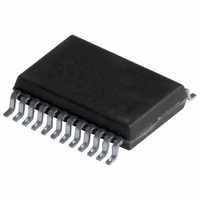
74LVC823ADB,112 NXP Semiconductors, 74LVC823ADB,112 Datasheet

74LVC823ADB,112
Specifications of 74LVC823ADB,112
74LVC823ADB
935262540112
Related parts for 74LVC823ADB,112
74LVC823ADB,112 Summary of contents
Page 1
D-type flip-flop with 5 V tolerant inputs/outputs; positive edge-trigger; 3-state Rev. 02 — 10 May 2004 1. General description The 74LVC823A is a high performance, low-power, low-voltage Si-gate CMOS device and superior to most advanced CMOS compatible TTL ...
Page 2
Philips Semiconductors 3. Quick reference data Table 1: GND = Symbol Parameter t , PHL t PLH t PHL f max [ input frequency in ...
Page 3
Philips Semiconductors 5. Functional diagram Fig 1. Functional diagram. Fig 2. Logic symbol. 9397 750 13128 Product data sheet 9-bit D-type flip-flop with 5 V tolerant inputs/outputs FF0 FF8 ...
Page 4
Philips Semiconductors Fig 4. Logic diagram. 9397 750 13128 Product data sheet 9-bit D-type flip-flop with 5 V tolerant inputs/outputs FF0 FF1 ...
Page 5
Philips Semiconductors 6. Pinning information 6.1 Pinning 823 GND 12 Fig 5. Pin configuration SO24 and (T)SSOP24. 6.2 ...
Page 6
Philips Semiconductors Table 3: Symbol Functional description 7.1 Function table Table 4: Operating mode Clear Load and read register Load register and disable outputs Hold [ HIGH voltage level; h ...
Page 7
Philips Semiconductors 8. Limiting values Table 5: In accordance with the Absolute Maximum Rating System (IEC 60134). Voltages are referenced to GND (ground = 0 V). Symbol Parameter ...
Page 8
Philips Semiconductors 10. Static characteristics Table 7: Static characteristics At recommended operating conditions; voltages are referenced to GND (ground = 0 V). Symbol Parameter [ +85 C amb V HIGH-level input voltage IH V LOW-level ...
Page 9
Philips Semiconductors Table 7: Static characteristics At recommended operating conditions; voltages are referenced to GND (ground = 0 V). Symbol Parameter I 3-state output OFF-state OZ current I power-off leakage supply off I quiescent supply current CC I additional quiescent ...
Page 10
Philips Semiconductors Table 8: Dynamic characteristics GND = 0 V; see Figure 11 for test circuit. Symbol Parameter t set-up time set-up time removal time MR rem t hold time Dn to ...
Page 11
Philips Semiconductors Table 8: Dynamic characteristics GND = 0 V; see Figure 11 for test circuit. Symbol Parameter t clock pulse width HIGH or LOW W master reset pulse width HIGH or LOW see t set-up time ...
Page 12
Philips Semiconductors 12. Waveforms Fig 7. Clock to output propagation delays, clock pulse width and maximum clock pulse Fig 8. Data set-up and hold times for data and clock enable inputs to clock input. 9397 750 13128 Product data sheet ...
Page 13
Philips Semiconductors Fig 9. Master reset pulse width, master reset to clock removal time and master reset to Table 9: Supply voltage V CC 1.2 V 2 3.6 V 9397 750 13128 Product data sheet 9-bit ...
Page 14
Philips Semiconductors Fig 10. 3-state outputs enable and disable times. Table 10: Supply voltage V CC 1.2 V 2 3.6 V 9397 750 13128 Product data sheet 9-bit D-type flip-flop with 5 V tolerant inputs/outputs V ...
Page 15
Philips Semiconductors Fig 11. Load circuitry for switching times. Table 11: Supply voltage V CC 1.2 V 2 3.6 V [1] The circuit performs better when R 9397 750 13128 Product data sheet 9-bit D-type flip-flop ...
Page 16
Philips Semiconductors 13. Package outline SO24: plastic small outline package; 24 leads; body width 7 pin 1 index 1 e DIMENSIONS (inch dimensions are derived from the original mm dimensions) A UNIT ...
Page 17
Philips Semiconductors SSOP24: plastic shrink small outline package; 24 leads; body width 5 pin 1 index 1 DIMENSIONS (mm are the original dimensions) A UNIT max. 0.21 1. ...
Page 18
Philips Semiconductors TSSOP24: plastic thin shrink small outline package; 24 leads; body width 4 pin 1 index 1 DIMENSIONS (mm are the original dimensions) A UNIT max. 0.15 0.95 mm ...
Page 19
Philips Semiconductors DHVQFN24: plastic dual in-line compatible thermal enhanced very thin quad flat package; no leads; 24 terminals; body 3.5 x 5.5 x 0.85 mm terminal 1 index area terminal 1 index area ...
Page 20
Philips Semiconductors 14. Revision history Table 12: Revision history Document ID Release date 74LVC823A_2 20040510 • Modifications: The format of this data sheet has been redesigned to comply with the current presentation and information standard of Philips Semiconductors. • Table ...
Page 21
Philips Semiconductors 15. Data sheet status [1] Level Data sheet status Product status I Objective data Development II Preliminary data Qualification III Product data Production [1] Please consult the most recently issued data sheet before initiating or completing a design. ...
Page 22
Philips Semiconductors 19. Contents 1 General description . . . . . . . . . . . . . . . . . . . . . . 1 2 Features . . . . . . . . ...


