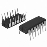
MC74AC00NG ON Semiconductor, MC74AC00NG Datasheet

MC74AC00NG
Specifications of MC74AC00NG
MC74AC00NGOS
Related parts for MC74AC00NG
MC74AC00NG Summary of contents
Page 1
MC74AC00, MC74ACT00 Quad 2−Input NAND Gate High−Performance Silicon−Gate CMOS Features • Output Drive Capability: $24 mA • Operating Voltage Range AC00; 4.5 to 5.5 ACT00 • Low Input Current: 1.0 mA • High Noise Immunity Characteristic ...
Page 2
MAXIMUM RATINGS Symbol V DC Supply Voltage Input Voltage Output Voltage Input Diode Current Output Diode Current Output Sink/Source Current Supply Current ...
Page 3
DC CHARACTERISTICS V CC (V) Symbol Parameter V Minimum High Level 3.0 IH Input Voltage 4.5 5.5 V Maximum Low Level 3.0 IL Input Voltage 4.5 5.5 V Minimum High Level 3.0 OH Output Voltage 4.5 5.5 3.0 4.5 5.5 ...
Page 4
DC CHARACTERISTICS V CC (V) Symbol Parameter V Minimum High Level 4.5 IH Input Voltage 5.5 V Maximum Low Level 4.5 IL Input Voltage 5.5 V Minimum High Level 4.5 OH Output Voltage 5.5 4.5 5.5 V Maximum Low Level ...
Page 5
INPUT 10% t PLH OUTPUT Y 50% Figure 3. Switching Waveforms OUTPUT INPUT DEVICE UNDER TEST *Includes all probe and jig capacitance Figure 4. Test Circuit http://onsemi.com GND ...
Page 6
... ORDER INFORMATION Device MC74AC00D MC74AC00DG MC74AC00N MC74AC00NG MC74AC00DR2 MC74AC00DR2G MC74AC00DTR2 MC74AC00DTR2G MC74AC00MEL MC74AC00MELG MC74ACT00N MC74ACT00NG MC74ACT00D MC74ACT00DG MC74ACT00DR2 MC74ACT00DR2G MC74ACT00DTR2 MC74ACT00DTR2G MC74ACT00MEL MC74ACT00MELG †For information on tape and reel specifications, including part orientation and tape sizes, please refer to our Tape and Reel Packaging Specifications Brochure, BRD8011/D. *This package is inherently Pb− ...
Page 7
... G −T− SEATING 14 PL PLANE 0.25 (0.010 14X 0.58 *For additional information on our Pb−Free strategy and soldering details, please download the ON Semiconductor Soldering and Mounting Techniques Reference Manual, SOLDERRM/D. PACKAGE DIMENSIONS SOIC−14 CASE 751A−03 ISSUE 0.25 (0.010 ...
Page 8
−T− SEATING PLANE 0.13 (0.005) PDIP−14 CASE 646−06 ISSUE http://onsemi.com 8 NOTES: 1. DIMENSIONING AND TOLERANCING PER ANSI Y14.5M, 1982. ...
Page 9
... S A −V− C 0.10 (0.004) −T− SEATING G D PLANE 14X 0.36 *For additional information on our Pb−Free strategy and soldering details, please download the ON Semiconductor Soldering and Mounting Techniques Reference Manual, SOLDERRM/D. PACKAGE DIMENSIONS TSSOP−14 CASE 948G−01 ISSUE 0.25 (0.010) ...
Page 10
... Opportunity/Affirmative Action Employer. This literature is subject to all applicable copyright laws and is not for resale in any manner. PUBLICATION ORDERING INFORMATION LITERATURE FULFILLMENT: Literature Distribution Center for ON Semiconductor P.O. Box 5163, Denver, Colorado 80217 USA Phone: 303−675−2175 or 800−344−3860 Toll Free USA/Canada Fax: 303− ...


