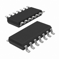
HEF4081BT,653 NXP Semiconductors, HEF4081BT,653 Datasheet - Page 6

HEF4081BT,653
Manufacturer Part Number
HEF4081BT,653
Description
IC 2IN AND GATE QUAD 14SOIC
Manufacturer
NXP Semiconductors
Series
4000Br
Datasheet
1.HEF4081BP652.pdf
(11 pages)
Specifications of HEF4081BT,653
Number Of Circuits
4
Package / Case
14-SOIC (3.9mm Width), 14-SOL
Logic Type
AND Gate
Number Of Inputs
2
Current - Output High, Low
4.2mA, 4.2mA
Voltage - Supply
3 V ~ 15 V
Operating Temperature
-40°C ~ 125°C
Mounting Type
Surface Mount
Product
AND
Logic Family
HEF4000
High Level Output Current
- 3.6 mA
Low Level Output Current
3.6 mA
Propagation Delay Time
20 ns
Supply Voltage (max)
15.5 V
Supply Voltage (min)
3 V
Maximum Operating Temperature
+ 125 C
Mounting Style
SMD/SMT
Minimum Operating Temperature
- 40 C
Logical Function
AND
Number Of Elements
4
Operating Supply Voltage (typ)
3.3/5/9/12V
Operating Temp Range
-40C to 125C
Package Type
SO
Number Of Outputs
1
Technology
CMOS
Mounting
Surface Mount
Pin Count
14
Operating Temperature Classification
Automotive
Quiescent Current
1uA
Operating Supply Voltage (max)
15V
Operating Supply Voltage (min)
3V
Lead Free Status / RoHS Status
Lead free / RoHS Compliant
Lead Free Status / RoHS Status
Lead free / RoHS Compliant, Lead free / RoHS Compliant
Other names
933373090653
HEF4081BTD-T
HEF4081BTD-T
HEF4081BTD-T
HEF4081BTD-T
Available stocks
Company
Part Number
Manufacturer
Quantity
Price
Part Number:
HEF4081BT,653
Manufacturer:
NXP/恩智浦
Quantity:
20 000
NXP Semiconductors
11. Waveforms
Table 9.
Table 10.
HEF4081B_6
Product data sheet
Supply voltage
V
5 V to 15 V
Supply voltage
V
5 V to 15 V
Fig 4.
Fig 5.
DD
DD
Measurement points are given in
Logic levels: V
Input to output propagation delay and output transition times
Test data is given in
Definitions for test circuit:
DUT = Device Under Test.
C
R
Test circuit
L
T
Measurement points
Test data
= load capacitance including jig and probe capacitance.
= termination resistance should be equal to the output impedance Z
OL
and V
Table
Input
V
V
OH
I
SS
are typical output voltage levels that occur with the output load.
10.
or V
nA, nB input
nY output
DD
Table
Input
V
0.5V
G
M
9.
V
V
DD
0 V
OH
OL
V
V
Rev. 06 — 2 December 2009
I
I
10 %
R T
10 %
DUT
V
V
90 %
DD
M
t
r
t
≤ 20 ns
V
90 %
r
t
M
, t
PLH
t
TLH
f
V
O
C L
o
of the pulse generator.
001aag182
t
f
001aai140
t
PHL
t
THL
V
0.5V
Output
M
DD
Load
C
50 pF
L
Quad 2-input AND gate
HEF4081B
© NXP B.V. 2009. All rights reserved.
6 of 11


