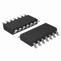
MC14071BDR2 ON Semiconductor, MC14071BDR2 Datasheet - Page 7

MC14071BDR2
Manufacturer Part Number
MC14071BDR2
Description
IC GATE OR QUAD CMOS 14SOIC
Manufacturer
ON Semiconductor
Series
4000Br
Datasheet
1.MC14011BDR2G.pdf
(14 pages)
Specifications of MC14071BDR2
Logic Type
OR Gate
Number Of Inputs
2
Number Of Circuits
4
Current - Output High, Low
3.4mA, 3.4mA
Voltage - Supply
3 V ~ 18 V
Operating Temperature
-55°C ~ 125°C
Mounting Type
Surface Mount
Package / Case
14-SOIC (3.9mm Width), 14-SOL
Lead Free Status / RoHS Status
Contains lead / RoHS non-compliant
Other names
MC14071BDR2OSCT
Available stocks
Company
Part Number
Manufacturer
Quantity
Price
Part Number:
MC14071BDR2
Manufacturer:
ON/安森美
Quantity:
20 000
Part Number:
MC14071BDR2G
Manufacturer:
ON/安森美
Quantity:
20 000
5.0
4.0
3.0
2.0
1.0
8.0
6.0
4.0
2.0
16
14
12
10
0
0
0
0
1.0
2.0
Figure 10. V
2.0
4.0
Figure 8. V
V
V
V
V
O
O
out
V
in
in
, INPUT VOLTAGE (Vdc)
3.0
, INPUT VOLTAGE (Vdc)
6.0
0
SINGLE INPUT NAND, AND
MULTIPLE INPUT NOR, OR
(a) Inverting Function
V
TYPICAL B−SERIES GATE CHARACTERISTICS (cont’d)
SINGLE INPUT NOR, OR
MULTIPLE INPUT NAND, AND
DD
DD
4.0
DD
8.0
= 15 Vdc
V
= 5.0 Vdc
IL
SINGLE INPUT NOR, OR
MULTIPLE INPUT NAND, AND
SINGLE INPUT NAND, AND
MULTIPLE INPUT NOR, OR
5.0
10
VOLTAGE TRANSFER CHARACTERISTICS
V
Figure 11. DC Noise Immunity
IH
http://onsemi.com
V
V
DD
in
V
SS
= 0 VOLTS DC
7
from an ideal “1” or “0” input level which does not produce
output state change(s). The typical and guaranteed limit
values of the input values V
be at a fixed voltage V
Characteristics table. V
in Figure 11.
“0” levels =
The DC noise margin is defined as the input voltage range
Guaranteed minimum noise margins for both the “1” and
V
V
V
O
O
out
8.0
6.0
4.0
2.0
10
0
(b) Non−Inverting Function
0
0
1.0 V with a 5.0 V supply
2.0 V with a 10.0 V supply
2.5 V with a 15.0 V supply
V
DD
2.0
V
IL
4.0
DC NOISE MARGIN
Figure 9. V
V
IL
in
, INPUT VOLTAGE (Vdc)
6.0
and V
V
O
IH
SINGLE INPUT NAND, AND
MULTIPLE INPUT NOR, OR
IL
are given in the Electrical
SINGLE INPUT NOR, OR
MULTIPLE INPUT NAND, AND
and V
IH
8.0
DD
V
V
are presented graphically
DD
in
= 10 Vdc
IH
10
for the output(s) to


