MM74HC259M Fairchild Semiconductor, MM74HC259M Datasheet
MM74HC259M
Manufacturer Part Number
MM74HC259M
Description
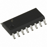
IC LATCH ADDRESS 8BIT 16-SOIC
Manufacturer
Fairchild Semiconductor
Series
74HCr
Specifications of MM74HC259M
Logic Type
D-Type, Addressable
Circuit
1:8
Output Type
Standard
Voltage - Supply
2 V ~ 6 V
Independent Circuits
1
Delay Time - Propagation
17ns
Current - Output High, Low
5.2mA, 5.2mA
Operating Temperature
-40°C ~ 85°C
Mounting Type
Surface Mount
Package / Case
16-SOIC (3.9mm Width)
Lead Free Status / RoHS Status
Lead free / RoHS Compliant
Available stocks
Company
Part Number
Manufacturer
Quantity
Price

Part Number:
MM74HC259M
Manufacturer:
FAIRCHILD/仙童
Quantity:
20 000
Company:
Part Number:
MM74HC259MX
Manufacturer:
FAIRCHIL
Quantity:
2 146


© 1999 Fairchild Semiconductor Corporation
Order Number
MM74HC259M
MM74HC259SJ
MM74HC259MTC
MM74HC259N
MM74HC259
8-Bit Addressable Latch/3-to-8 Line Decoder
General Description
The MM74HC259 device utilizes advanced silicon-gate
CMOS technology to implement an 8-bit addressable latch,
designed for general purpose storage applications in digital
systems.
The MM74HC259 has a single data input (D), 8 latch out-
puts (Q1–Q8), 3 address inputs (A, B, and C), a common
enable input (G), and a common CLEAR input. To operate
this device as an addressable latch, data is held on the D
input, and the address of the latch into which the data is to
be entered is held on the A, B, and C inputs. When
ENABLE is taken LOW the data flows through to the
addressed output. The data is stored when ENABLE transi-
tions from LOW-to-HIGH. All unaddressed latches will
remain unaffected. With enable in the HIGH state the
device is deselected, and all latches remain in their previ-
ous state, unaffected by changes on the data or address
Ordering Code:
Devices also available in Tape and Reel. Specify by appending the suffix letter “X” to the ordering code.
Connection Diagram
Pin Assignments for DIP, SOIC, SOP and TSSOP
Package Number Package Description
MTC16
Top View
M16D
M16A
N16E
16-Lead Small Outline Integrated Circuit (SOIC), JEDEC MS-120, 0.150” Narrow
16-Lead Small Outline Package (SOP), EIAJ TYPE II, 5.3mm Wide
16-Lead Thin Shrink Small Outline Package (TSSOP), JEDEC MO-153, 4.4mm Wide
16-Lead Plastic Dual-In-Line Package (PDIP), JEDEC MS-001, 0.300” Wide
DS005006.prf
inputs. To eliminate the possibility of entering erroneous
data into the latches, the enable should be held HIGH
(inactive) while the address lines are changing.
If enable is held HIGH and CLEAR is taken LOW all eight
latches are cleared to a LOW state. If enable is LOW all
latches except the addressed latch will be cleared. The
addressed latch will instead follow the D input, effectively
implementing a 3-to-8 line decoder.
All inputs are protected from damage due to static dis-
charge by diodes to V
Features
Latch Selection Table
H
D
Q
before the indicated steady-state input
conditions were established.
i0
Typical propagation delay: 18 ns
Wide supply range: 2–6V
Low input current: 1 A maximum
Low quiescent current: 80 A maximum (74HC Series)
the level of Q
HIGH level, L
the level at the data input
C
H
H
H
H
L
L
L
L
i
Select Inputs
(i
LOW level
0, 1 .. .7, as appropriate)
B
H
H
H
H
L
L
L
L
CC
and ground.
A
H
H
H
H
L
L
L
L
September 1983
Revised February 1999
Addressed
www.fairchildsemi.com
Latch
0
1
2
3
4
5
6
7
Related parts for MM74HC259M
Image
Part Number
Description
Manufacturer
Datasheet
Request
R

Part Number:
Description:
Fairchild Semiconductor [IGBT MODULE]
Manufacturer:
Fairchild Semiconductor
Datasheet:

Part Number:
Description:
Discrete Semiconductor Modules
Manufacturer:
Fairchild Semiconductor
Part Number:
Description:
Discrete Semiconductor Modules
Manufacturer:
Fairchild Semiconductor
Part Number:
Description:
This N-Channel MOSFET is produced using Fairchild Semiconductor�s advanced Power Trench� process
Manufacturer:
Fairchild Semiconductor
Datasheet:
Part Number:
Description:
This N-Channel MOSFET is produced using Fairchild Semiconductor�s advanced Power Trench� process
Manufacturer:
Fairchild Semiconductor
Datasheet:
Part Number:
Description:
This N-Channel MOSFET is produced using Fairchild Semiconductor�s advanced PowerTrench� process
Manufacturer:
Fairchild Semiconductor
Datasheet:
Part Number:
Description:
This N-Channel MOSFET is produced using Fairchild Semiconductor�s advanced PowerTrench� process
Manufacturer:
Fairchild Semiconductor
Datasheet:
Part Number:
Description:
This N-Channel MOSFET is produced using Fairchild Semiconductor�s advanced Power Trench� process
Manufacturer:
Fairchild Semiconductor
Datasheet:
Part Number:
Description:
This N-Channel logic Level MOSFETs are produced using Fairchild Semiconductor�s advanced Power Trench� process that has been special tailored to minimize the on-state resistance and yet maintain superior switching performance
Manufacturer:
Fairchild Semiconductor
Datasheet:
Part Number:
Description:
This N-Channel MOSFET is produced using Fairchild Semiconductor�s advanced Power Trench� process
Manufacturer:
Fairchild Semiconductor
Datasheet:
Part Number:
Description:
This N-Channel SyncFET� is produced using Fairchild Semiconductor�s advanced PowerTrench� process
Manufacturer:
Fairchild Semiconductor
Datasheet:
Part Number:
Description:
This N-Channel SyncFET� is produced using Fairchild Semiconductor�s advanced PowerTrench� process
Manufacturer:
Fairchild Semiconductor
Datasheet:
Part Number:
Description:
This N-Channel SyncFET� is produced using Fairchild Semiconductor�s advanced PowerTrench� process
Manufacturer:
Fairchild Semiconductor
Datasheet:
Part Number:
Description:
This N-Channel logic Level MOSFETs are produced using Fairchild Semiconductor�s advanced Power Trench� process that has been special tailored to minimize the on-state resistance and yet maintain superior switching performance
Manufacturer:
Fairchild Semiconductor
Datasheet: